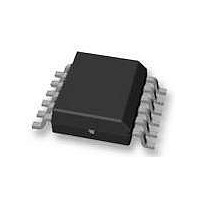
VN5050J-E STMicroelectronics, VN5050J-E Datasheet - Page 20

VN5050J-E
Manufacturer Part Number
VN5050J-E
Description
IC DRVR HIGHSIDE AUTO PWRSSO-12
Manufacturer
STMicroelectronics
Type
High Sider
Datasheet
1.VN5050JTR-E.pdf
(31 pages)
Specifications of VN5050J-E
Input Type
Non-Inverting
Number Of Outputs
1
On-state Resistance
50 mOhm
Current - Peak Output
19A
Voltage - Supply
4.5 V ~ 36 V
Operating Temperature
-40°C ~ 150°C
Mounting Type
Surface Mount
Package / Case
PowerSSO-12
Product
Driver ICs - Various
Supply Voltage (max)
36 V
Supply Voltage (min)
4.5 V
Supply Current
0.005 mA
Maximum Operating Temperature
+ 150 C
Mounting Style
SMD/SMT
Maximum Turn-off Delay Time
35000 ns
Maximum Turn-on Delay Time
20000 ns
Minimum Operating Temperature
- 40 C
Number Of Drivers
1
Device Type
High Side
Module Configuration
High Side
Peak Output Current
19A
Output Resistance
0.065ohm
Input Delay
20µs
Output Delay
35µs
Supply Voltage Range
4.5V To 36V
Rohs Compliant
Yes
Lead Free Status / RoHS Status
Lead free / RoHS Compliant
Current - Output / Channel
-
Lead Free Status / Rohs Status
Lead free / RoHS Compliant
Available stocks
Company
Part Number
Manufacturer
Quantity
Price
Part Number:
VN5050J-E
Manufacturer:
ST
Quantity:
20 000
Application information
3
3.1
3.1.1
20/31
Application information
Figure 27. Application schematic
GND protection network against reverse battery
Solution 1: resistor in the ground line (R
This can be used with any type of load.
The following is an indication on how to dimension the R
1.
2.
where -I
maximum rating section of the device datasheet.
Power Dissipation in R
P
This resistor can be shared amongst several different HSDs. Please note that the value of
this resistor should be calculated with formula (1) where I
maximum on-state currents of the different devices.
Please note that if the microprocessor ground is not shared by the device ground then the
R
values. This shift will vary depending on how many devices are ON in the case of several
high side drivers sharing the same R
If the calculated power dissipation leads to a large resistor or several devices have to share
the same resistor then ST suggests to utilize Solution 2 (see below).
D
GND
= (-V
R
R
will produce a shift (I
GND
GND
CC
GND
+5V
µC
)
≤ 600mV / (I
≥ (− V
2
/R
is the DC reverse ground pin current and can be found in the absolute
GND
CC
) / (-I
R
R
R
prot
prot
prot
S(on)max
GND
GND
S(on)max
+5V
)
(when V
).
STATUS
STAT_DIS
INPUT
* R
CC
GND
<0: during reverse battery situations) is:
GND
.
) in the input thresholds and the status output
V
GND
GND
R
GND
GND
GND
S(on)max
only)
V
CC
resistor.
D
GND
becomes the sum of the
OUTPUT
VN5050J-E
D
ld


