VN820PT-E STMicroelectronics, VN820PT-E Datasheet - Page 10
VN820PT-E
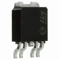
Manufacturer Part Number
VN820PT-E
Description
IC DRIVER HIGH SIDE 9A PPAK
Manufacturer
STMicroelectronics
Type
High Sider
Datasheet
1.VN820PT-E.pdf
(44 pages)
Specifications of VN820PT-E
Input Type
Non-Inverting
Number Of Outputs
1
On-state Resistance
40 mOhm
Current - Output / Channel
9A
Voltage - Supply
5.5 V ~ 36 V
Operating Temperature
-40°C ~ 150°C
Mounting Type
Surface Mount
Package / Case
PPAK (4 leads + tab)
Supply Voltage (min)
5.5 V
Supply Current
3.5 mA
Maximum Power Dissipation
65800 mW
Maximum Operating Temperature
+ 150 C
Mounting Style
SMD/SMT
Maximum Turn-off Delay Time
30000 ns
Maximum Turn-on Delay Time
30000 ns
Minimum Operating Temperature
- 40 C
Number Of Drivers
1
Device Type
High Side
Module Configuration
High Side
Peak Output Current
9A
Output Resistance
0.04ohm
Input Delay
30µs
Output Delay
30µs
Supply Voltage Range
5.5V To 36V
Driver Case Style
PPAK
Rohs Compliant
Yes
Driver Configuration
Non-Inverting
Driver Type
High Side
Input Logic Level
CMOS
Operating Supply Voltage (max)
36V
Power Dissipation
65.8W
Operating Supply Voltage (min)
5.5V
Operating Supply Voltage (typ)
13V
Turn Off Delay Time
30us
Turn On Delay Time (max)
30us
Operating Temp Range
-40C to 150C
Operating Temperature Classification
Automotive
Mounting
Surface Mount
Pin Count
4 +Tab
Package Type
PPAK
Lead Free Status / RoHS Status
Lead free / RoHS Compliant
Current - Peak Output
-
Lead Free Status / Rohs Status
Lead free / RoHS Compliant
Available stocks
Company
Part Number
Manufacturer
Quantity
Price


Electrical specifications
2.3
10/44
Electrical characteristics
Values specified in this section are for 8 V < V
otherwise stated.
Table 5.
Table 6.
dV
dV
V
Symbol
I
I
I
I
V
USDhyst
Symbol
L(off1)
L(off2)
L(off3)
L(off4)
R
V
V
OUT
OUT
USD
I
t
t
CC
OV
ON
S
d(on)
d(off)
/dt
/dt
(on)
(off)
Operating supply voltage
Undervoltage shutdown
Undervoltage shutdown
hysteresis
Overvoltage shutdown
On-state resistance
Supply current
Off-state output current
Off-state output current
Off-state output current
Off-state output current
Power
Switching (V
Turn-on delay time
Turn-off delay time
Turn-on voltage slope
Turn-off voltage slope
Parameter
Parameter
CC
= 13 V)
Doc ID 10890 Rev 6
I
I
Off-state; V
V
Off-state; V
V
On-state; V
I
V
V
V
T
V
T
R
V
R
V
R
V
R
V
OUT
OUT
OUT
j
j
IN
IN
IN
IN
IN
IN
OUT
OUT
OUT
OUT
L
L
L
L
= 125°C
= 25 °C
= 4.3
= 4.3
= 4.3
= 4.3
= V
= V
= V
= 0 V; V
= V
= V
= 3 A; T
= 3 A; V
= 0 A
=10.4 V
= 1.3 V
= 11.7 V
= 1.3 V
OUT
OUT
OUT
OUT
OUT
Test conditions
Test conditions
from V
from V
from V
from V
CC
CC
CC
= 0 V
= 0 V; T
= 0 V
= 0 V; V
= 0 V; V
OUT
CC
j
CC
= 25 °C; V
= 13 V;
= 13 V;
= 13 V; V
= 3.5 V
> 8 V
< 36 V; -40 °C < T
IN
OUT
OUT
IN
j
CC
CC
=
falling edge to
rising edge to
25
= 1.3 V to
= 11.7 V to
= 13 V;
= 13 V;
IN
CC
°C
= 5 V;
> 8 V
j
Min.
Min.
< 150 °C, unless
-75
5.5
36
3
0
See
See
Figure 21
Figure 22
Typ.
Typ.
30
30
0.5
13
10
10
4
2
Max. Unit
Max. Unit
5.5
3.5
36
40
80
25
20
50
0
5
3
VN820-E
V/µs
V/µs
m
m
mA
µA
µA
µA
µA
µA
µA
µs
µs
V
V
V
V
Related parts for VN820PT-E
Image
Part Number
Description
Manufacturer
Datasheet
Request
R

Part Number:
Description:
IC DRVR HI SIDE 9A AUTO P2PAK
Manufacturer:
STMicroelectronics
Datasheet:

Part Number:
Description:
IC DVR HI SIDE 9A AUTO PENTAWATT
Manufacturer:
STMicroelectronics
Datasheet:
Part Number:
Description:
IC DRIVER HIGHSIDE 9A PENTAWATT5
Manufacturer:
STMicroelectronics
Datasheet:

Part Number:
Description:
IC DRIVER HIGH SIDE 9A PENTAWAT5
Manufacturer:
STMicroelectronics
Datasheet:
Part Number:
Description:
IC DRIVER HI SIDE 9A PENTAWATT-5
Manufacturer:
STMicroelectronics
Datasheet:
Part Number:
Description:
IC DRIVER HIGHSIDE 9A P2PAK-4
Manufacturer:
STMicroelectronics
Datasheet:
Part Number:
Description:
IC DRIVER HI SIDE 9A PENTAWATT-5
Manufacturer:
STMicroelectronics
Datasheet:
Part Number:
Description:
IC DRIVER HIGH SIDE 9A PENTAWAT5
Manufacturer:
STMicroelectronics
Datasheet:
Part Number:
Description:
STMicroelectronics [RIPPLE-CARRY BINARY COUNTER/DIVIDERS]
Manufacturer:
STMicroelectronics
Datasheet:
Part Number:
Description:
STMicroelectronics [LIQUID-CRYSTAL DISPLAY DRIVERS]
Manufacturer:
STMicroelectronics
Datasheet:

Part Number:
Description:
BOARD EVAL FOR MEMS SENSORS
Manufacturer:
STMicroelectronics
Datasheet:
Part Number:
Description:
NPN TRANSISTOR POWER MODULE
Manufacturer:
STMicroelectronics
Datasheet: