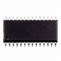
VNQ830-E STMicroelectronics, VNQ830-E Datasheet - Page 6

VNQ830-E
Manufacturer Part Number
VNQ830-E
Description
IC DRIVER HISIDE QUAD 28-SOIC
Manufacturer
STMicroelectronics
Type
High Sider
Datasheet
1.VNQ830TR-E.pdf
(21 pages)
Specifications of VNQ830-E
Input Type
Non-Inverting
Number Of Outputs
4
On-state Resistance
65 mOhm
Current - Peak Output
9A
Voltage - Supply
5.5 V ~ 36 V
Mounting Type
Surface Mount
Package / Case
28-SOIC (7.5mm Width)
Supply Voltage (min)
5.5 V
Supply Current
0.012 mA
Maximum Power Dissipation
6250 mW
Maximum Operating Temperature
+ 150 C
Mounting Style
SMD/SMT
Minimum Operating Temperature
- 40 C
Device Type
High Side
Module Configuration
High Side
Peak Output Current
9A
Output Resistance
0.065ohm
Input Delay
30µs
Output Delay
30µs
Supply Voltage Range
5.5V To 36V
Driver Case Style
SOIC
Rohs Compliant
Yes
Lead Free Status / RoHS Status
Lead free / RoHS Compliant
Operating Temperature
-
Current - Output / Channel
-
Lead Free Status / Rohs Status
Lead free / RoHS Compliant
Available stocks
Company
Part Number
Manufacturer
Quantity
Price
VNQ830-E
ELECTRICAL CHARACTERISTICS (continued)
Table 8. Status Pin (Per each channel)
Table 9. Switching (Per each channel) (V
Table 10. Openload Detection (Per each channel)
Table 11. Logic Input (Per each channel)
6/21
dV
dV
Symbol
V
I
C
Symbol
Symbol
LSTAT
V
t
t
Symbol
DOL(on)
DOL(off)
OUT
OUT
V
STAT
STAT
SCL
t
t
V
V
I
V
I(hyst)
d(on)
d(off)
V
I
OL
I
OL
IH
ICL
IL
IH
IL
/dt
/dt
(on)
(off)
Status Low Output Voltage I
Status Leakage Current
Status Pin Input
Capacitance
Status Clamp Voltage
Openload ON State
Detection Threshold
Openload ON State
Detection Delay
Openload OFF State
Voltage Detection
Threshold
Openload Detection Delay
at Turn Off
Input Low Level
Low Level Input Current V
Input High Level
High Level Input Current V
Input Hysteresis Voltage
Input Clamp Voltage
Turn-on Delay Time
Turn-off Delay Time
Turn-on Voltage Slope
Turn-off Voltage Slope
Parameter
Parameter
Parameter
Parameter
I
I
R
V
R
V
R
V
R
V
Normal Operation; V
Normal Operation; V
I
I
IN
IN
STAT
STAT
STAT
IN
IN
OUT
OUT
OUT
OUT
L
L
L
L
=1mA
=-1mA
V
I
=6.5
=6.5
=6.5
=6.5
V
=1.25V
=3.25V
OUT
IN
IN
=1.6mA
=1mA
=-1mA
=1.3V
=11.7V
=10.4V
=1.3V
=5V
=0V
=0A
CC
from V
from V
from V
from V
=13V)
Test Conditions
Test Conditions
Test Conditions
Test Conditions
IN
IN
OUT
OUT
rising edge to
falling edge to
=1.3V to
=11.7V to
STAT
STAT
=5V
=5V
3.25
Min
Min
Min
0.5
1
6
6
Min
1.5
50
diagram
diagram
relative
relative
Typ
-0.7
Typ
See
See
Typ
6.8
-0.7
30
30
6.8
Typ
100
2.5
Max
1000
Max
1.25
Max
Max
100
200
200
0.5
3.5
10
10
8
8
Unit
V/ s
V/ s
Unit
Unit
Unit
mA
pF
V
V
V
V
V
V
V
V
V
A
s
s
A
A
s
s


