L6376D STMicroelectronics, L6376D Datasheet - Page 10
L6376D
Manufacturer Part Number
L6376D
Description
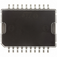
IC IPS QUAD 0.5A 20-POWERSOIC
Manufacturer
STMicroelectronics
Type
High Sider
Datasheet
1.L6376D013TR.pdf
(18 pages)
Specifications of L6376D
Input Type
Non-Inverting
Number Of Outputs
4
Current - Output / Channel
500mA
Current - Peak Output
900mA
Voltage - Supply
9.5 V ~ 35 V
Operating Temperature
-25°C ~ 85°C
Mounting Type
Surface Mount
Package / Case
PowerSO-20 Exposed Bottom Pad
Lead Free Status / RoHS Status
Lead free / RoHS Compliant
On-state Resistance
-
Available stocks
Company
Part Number
Manufacturer
Quantity
Price

Part Number:
L6376D013TR
Manufacturer:
ST
Quantity:
20 000


Overtemperature protection (OVT)
5
6
7
10/18
Overtemperature protection (OVT)
If the chip temperature exceeds Θlim (measured in a central position in the chip) the chip
deactivates itself.
The following actions are taken:
●
●
Normal operation is resumed as soon as (typically after some seconds) the chip
temperature monitored goes back below Θ
The different thresholds with hysteretic behavior assure that no intermittent conditions can
be generated.
Undervoltage protection (UV)
The supply voltage is expected to range from 9.5 V to 35 V, even if its reference value is
considered to be 24 V. In this range the device operates correctly. Below 9.5 V the overall
system has to be considered not reliable. Consequently the supply voltage is monitored
continuously and a signal, called UV, is internally generated and used.
The signal is “on” as long as the supply voltage does not reach the upper internal threshold
of the Vs comparator V
Once the UV signal has been removed, the supply voltage must decrease below the lower
threshold (i.e. V
The hysteresis V
voltages that may have a superimposed ripple around the average value.
The UV signal switches off the outputs, but has no effect on the creation of the reference
voltages for the internal comparators, nor on the continuous operation of the charge-pump
circuits.
Diagnostic logic
The situations that are monitored and signalled with the DIAG output pin are:
●
●
●
The diagnostic signal is transmitted via an open drain output (for ease of wired-or
connection of several such signals) and a low level represents the presence of at least one
of the monitored conditions, mentioned above.
all the output stages are switched off;
the signal DIAG is activated (active low).
current limit (OVC) in action; there are 4 individual current limiting circuits, one per each
output; they limit the current that can be sunk from each output, to a typical value of
800 mA, equal for all of them;
under voltage (UV);
over temperature protection (OVT).
sth
shys
-V
shys
is provided to prevent intermittent operation of the device at low supply
sth
) before it is turned on again.
. The UV signal disappears above V
lim
-Θ
H
.
sth
.
L6376
Related parts for L6376D
Image
Part Number
Description
Manufacturer
Datasheet
Request
R

Part Number:
Description:
Power Switch ICs - Power Distribution 0.5A Intel Power Sw
Manufacturer:
STMicroelectronics
Datasheet:

Part Number:
Description:
STMicroelectronics [RIPPLE-CARRY BINARY COUNTER/DIVIDERS]
Manufacturer:
STMicroelectronics
Datasheet:
Part Number:
Description:
STMicroelectronics [LIQUID-CRYSTAL DISPLAY DRIVERS]
Manufacturer:
STMicroelectronics
Datasheet:

Part Number:
Description:
BOARD EVAL FOR MEMS SENSORS
Manufacturer:
STMicroelectronics
Datasheet:
Part Number:
Description:
NPN TRANSISTOR POWER MODULE
Manufacturer:
STMicroelectronics
Datasheet:
Part Number:
Description:
TURBOSWITCH ULTRA-FAST HIGH VOLTAGE DIODE
Manufacturer:
STMicroelectronics
Datasheet:
Part Number:
Description:
Manufacturer:
STMicroelectronics
Datasheet:
Part Number:
Description:
DIODE / SCR MODULE
Manufacturer:
STMicroelectronics
Datasheet:
Part Number:
Description:
DIODE / SCR MODULE
Manufacturer:
STMicroelectronics
Datasheet:
Part Number:
Description:
Search -----> STE16N100
Manufacturer:
STMicroelectronics
Datasheet:
Part Number:
Description:
Search ---> STE53NA50
Manufacturer:
STMicroelectronics
Datasheet:
Part Number:
Description:
NPN Transistor Power Module
Manufacturer:
STMicroelectronics
Datasheet: