NID5004NT4G ON Semiconductor, NID5004NT4G Datasheet
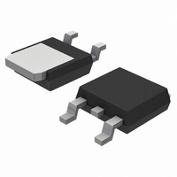
MOSFET N-CH 40V 6.5A DPAK

NID5004NT4G

Manufacturer Part Number
NID5004NT4G
Description
MOSFET N-CH 40V 6.5A DPAK
Manufacturer
ON Semiconductor
Series
HDPlus™r
Type
Low Sider
Datasheet

Specifications of NID5004NT4G

Input Type
Non-Inverting
Number Of Outputs
1
On-state Resistance
110 mOhm
Current - Peak Output
6.5A
Operating Temperature
-55°C ~ 150°C
Mounting Type
Surface Mount
Package / Case
DPak, TO-252 (2 leads+tab), SC-63
Rise Time
300 ns
Fall Time
750 ns
Supply Current
0.2 mA
Maximum Power Dissipation
1.3 W
Maximum Operating Temperature
+ 150 C
Mounting Style
SMD/SMT
Minimum Operating Temperature
- 55 C
Number Of Drivers
1
Lead Free Status / RoHS Status
Lead free / RoHS Compliant
Voltage - Supply
-
Current - Output / Channel
-
Lead Free Status / Rohs Status
Lead free / RoHS Compliant

Available stocks

Company
Part Number
Manufacturer
Quantity
Price
Part Number:
NID5004NT4G
Manufacturer:
ON/安森美
Quantity:
20 000
NID5004N
Self−Protected FET
with Temperature and
Current Limit
40 V, 6.5 A, Single N−Channel, DPAK
ON Semiconductor HDPlust technology.
MOSFET incorporates protection features such as integrated thermal
and current limits. The self−protected MOSFETs include an integrated
Drain−to−Gate Clamp that provides overvoltage protection from
transients and avalanche. The device is protected from Electrostatic
Discharge (ESD) by utilizing an integrated Gate−to−Source Clamp.
Features
Applications
© Semiconductor Components Industries, LLC, 2006
April, 2006 − Rev. 1
Self–protected FETs are a series of power MOSFETs which utilize
Short Circuit Protection
In Rush Current Limit
Thermal Shutdown with Automatic Restart
Avalanche Rated
Overvoltage Protection
ESD Protection (4 kV HBM)
Controlled Slew Rate for Low Noise Switching
AEC Q101 Qualified
This is a Pb−Free Device
Solenoid Driver
Relay Driver
Small Motors
Lighting
Relay Replacement
Load Switching
The self–protected
1
†For information on tape and reel specifications,
Gate
Input
NID5004NT4G
including part orientation and tape sizes, please
refer to our Tape and Reel Packaging Specification
Brochure, BRD8011/D.
D5004N = Device Code
Y
WW
G
(Clamped)
V
CASE 369C
40 V
Device
DSS
STYLE 2
ESD Protection
DPAK
ORDERING INFORMATION
= Year
= Work Week
= Pb−Free Device
Temperature
R
G
http://onsemi.com
Limit
110 mW @ 10 V
R
Overvoltage
(Pb−Free)
Protection
Package
DS(on)
DPAK
Publication Order Number:
Typ
Current
Limit
1
3
2500/Tape & Reel
2
1 = Gate
2 = Drain
3 = Source
MARKING
DIAGRAM
Shipping
Drain
NID5004N/D
(Limited)
Current
Sense
004NG
Source
I
YYW
6.5 A
D
D5
Typ

Related parts for NID5004NT4G

NID5004NT4G Summary of contents

Page 1

... CASE 369C STYLE 2 D5004N = Device Code Y = Year WW = Work Week G = Pb−Free Device ORDERING INFORMATION Device NID5004NT4G †For information on tape and reel specifications, including part orientation and tape sizes, please refer to our Tape and Reel Packaging Specification Brochure, BRD8011/D. 1 http://onsemi.com I Typ D R ...

Page 2

MOSFET MAXIMUM RATINGS (T = 25°C unless otherwise noted) J Rating Drain−to−Source Voltage Internally Clamped Gate−to−Source Voltage Drain Current Total Power Dissipation @ T = 25°C (Note 25°C (Note 2) A Thermal Resistance Junction−to−Case Junction−to−Ambient ...

Page 3

MOSFET ELECTRICAL CHARACTERISTICS Characteristic OFF CHARACTERISTICS Drain−to−Source Clamped Breakdown Voltage ( mA Zero Gate Voltage Drain Current ( Gate Input Current (V = ...

Page 4

5 DRAIN−TO−SOURCE VOLTAGE (VOLTS) DS Figure 1. On−Region Characteristics 0.15 0.14 0.13 0.12 0.11 0.10 3.0 4.0 5.0 6.0 7 GATE−TO−SOURCE VOLTAGE (VOLTS) GS Figure ...

Page 5

25° 0.1 0.2 0.3 0.4 0.5 0.6 0 SOURCE−TO−DRAIN VOLTAGE (VOLTS) SD Figure 7. Diode Forward Voltage vs. Current ...

Page 6

... ON Semiconductor Soldering and Mounting Techniques Reference Manual, SOLDERRM/D. N. American Technical Support: 800−282−9855 Toll Free USA/Canada Japan: ON Semiconductor, Japan Customer Focus Center 2−9−1 Kamimeguro, Meguro−ku, Tokyo, Japan 153−0051 Phone: 81−3−5773−3850 http://onsemi.com 6 ...

Related keywords