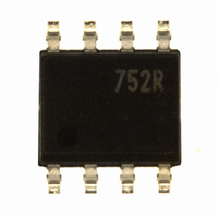
BSP752R Infineon Technologies, BSP752R Datasheet - Page 5

BSP752R
Manufacturer Part Number
BSP752R
Description
IC SWITCH HI SIDE POWER DSO-8
Manufacturer
Infineon Technologies
Series
miniPROFET®r
Type
High Sider
Specifications of BSP752R
Input Type
Non-Inverting
Number Of Outputs
1
On-state Resistance
150 mOhm
Current - Output / Channel
1.7A
Current - Peak Output
6.5A
Voltage - Supply
6 V ~ 52 V
Operating Temperature
-40°C ~ 150°C
Mounting Type
Surface Mount
Package / Case
DSO-8
Lead Free Status / RoHS Status
Lead free / RoHS Compliant
Other names
BSP752RINTR
BSP752RNT
BSP752RT
BSP752RT
BSP752RTINTR
BSP752RTINTR
BSP752RXT
SP000012796
SP000355392
BSP752RNT
BSP752RT
BSP752RT
BSP752RTINTR
BSP752RTINTR
BSP752RXT
SP000012796
SP000355392
Available stocks
Company
Part Number
Manufacturer
Quantity
Price
Part Number:
BSP752R
Manufacturer:
N/A
Quantity:
20 000
Electrical Characteristics
Parameter and Conditions
at T
Protection Functions
Initial peak short circuit current limit (pin 5 to 3)
T
T
T
T
Repetitive short circuit current limit
T
V
V
Output clamp (inductive load switch off)
at V
I
Overvoltage protection
I
Thermal overload trip temperature
Thermal hysteresis
Reverse Battery
Reverse battery
Drain-source diode voltage (V
T
bb
bb
1 Integrated protection functions are designed to prevent IC destruction under fault conditions
described in the data sheet. Fault conditions are considered as "outside" normal operating range.
Protection functions are not designed for continuous repetitive operation .
2 not subject to production test, specified by design
3 see also V ON(CL) in circuit diagram on page 8
4 Requires a 150
to be limited by the connected load. Power dissipation is higher compared to normal operating conditions due to the
voltage drop across the drain-source diode. The temperature protection is not active during reverse current operation!
Input current has to be limited (see max. ratings page 3).
j
j
j
j
j
j
bb
bb
= -40 °C, V
= 25 °C
= 150 °C
= -40...+150 °C, V
= T
= 150 °C
j
= 4 mA
= 4 mA
= -40...+150°C, V
OUT
< 40 V
> 40 V
jt
(see timing diagrams)
= V
bb
bb
resistor in GND connection. The reverse load current through the intrinsic drain-source diode has
- V
4)
= 20 V, t
ON(CL)
bb
bb
= 12..42V,
1)
> 40 V , ( see page 12 )
3)
,
m
= 150 µs
unless otherwise specified
OUT
> V
bb
)
Page 5
Symbol
I
I
V
V
T
-V
-V
L(SCp)
L(SCr)
T
ON(CL)
bb(AZ)
jt
bb
ON
jt
min.
150
59
62
4
-
-
-
-
-
-
-
-
Values
typ.
5
600
6.5
4.5
63
10
6
-
-
2)
-
-
-
max.
2004-01-27
52
9
-
-
-
-
-
-
-
-
-
-
BSP 752 R
Unit
A
V
°C
K
V
mV


