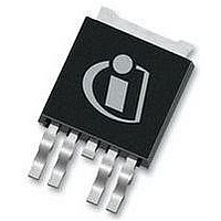
BTS6133D Infineon Technologies, BTS6133D Datasheet - Page 4

BTS6133D
Manufacturer Part Number
BTS6133D
Description
IC HIGH SIDE PWR SWITCH DPAK-5
Manufacturer
Infineon Technologies
Series
PROFET®r
Type
High Sider
Datasheet
1.BTS6133D.pdf
(17 pages)
Specifications of BTS6133D
Input Type
Non-Inverting
Number Of Outputs
1
On-state Resistance
8 mOhm
Current - Output / Channel
41A
Current - Peak Output
75A
Voltage - Supply
5.5 V ~ 38 V
Operating Temperature
-40°C ~ 150°C
Mounting Type
Surface Mount
Package / Case
DPak, TO-252 (4 leads + tab)
Power Load Switch Type
High Side
Input Voltage
38V
On Resistance Rds(on)
0.01ohm
Thermal Protection
ESD
Power Dissipation Pd
59W
No. Of Outputs
1
Internal Switch
No
Distribution Switch
RoHS Compliant
Current Limit
75A
On State Resistance
0.01ohm
Rohs Compliant
Yes
Distribution Switch Case Style
P-TO252-5
Lead Free Status / RoHS Status
Lead free / RoHS Compliant
Other names
BTS6133D
BTS6133DT
BTS6133DTR
BTS6133DXT
SP000014006
SP000274948
BTS6133DT
BTS6133DTR
BTS6133DXT
SP000014006
SP000274948
Available stocks
Company
Part Number
Manufacturer
Quantity
Price
Company:
Part Number:
BTS6133D
Manufacturer:
INF
Quantity:
7 500
Part Number:
BTS6133D
Manufacturer:
INFINEON/英飞凌
Quantity:
20 000
Parameter and Conditions
at T
Operating Parameters
Operating voltage (V
Undervoltage shutdown
Undervoltage restart of charge pump
Overvoltage protection
Standby current
Reverse Battery
Reverse battery voltage
On-state resistance (pin 1,5 to pin 3)
V
V
Integrated resistor in V
Inverse Load Current Operation
On-state resistance
Maximum transient inverse load current
Drain-source diode voltage
6)
7)
8)
9)
10)
Data Sheet
T j = 25 °C
T j = 85 °C
T j = 150 °C
(Pins 1,5 to Tab)
See diagram on page 10
I
I
V
I
bb
bb
bb
IN
L
bIN
j
= - 8V, V
= -12V, V
= 25, V
= - 7.5 A, I
V
Not subject to production test, specified by design.
See also V
For operation at voltages higher then |16V| please see required schematic on page 10.
Operation above these limits might cause a switch off of the device after the transition from inverse to
forward mode. In this case the device switches on again after a time delay of typ.1 msec.
=0
=15 mA
bIN
= 12 V, I
=V
bb
bb
-V
= 12 V unless otherwise specified
Z,IN
IN
IN
IN
IN
L
= 0, I
= 0, I
see schematic on page 8 and on page 14.
= 0, T
= - 7.5 A
in schematic on page 9.
L
L
IN
= -7.5 A, R
= -7.5 A, R
(Pins 1,5 to pin 3)
j
= 150°C
=0)
bb
8
)
6
9
)
)
line
7
)
(+V
out
IS
IS
T
> +V
= 1 kΩ,
= 1 kΩ, T
T
j
T
=-40...+150°C :
j
=-40...+120°C
7)
j
=-40...150 °C: V
bb
Page 4 of 17
)
T
7)
T
T
7)
T
j
T
j
j
T
=150 °C:
=150 °C:
= 150 °C:
7)
j
j
10
=150°C:
j
j
=25 °C:
=25 °C:
= 25 °C:
)
:
V
V
V
I
-V
R
R
R
- I
-V
Symbol
bb(off)
bb(on)
bIN(u)
bb(ucp)
Z,IN
ON(rev)
bb
ON(inv)
L(inv)
bb
ON
PROFET ® BTS 6133D
min
5.5
63
--
--
--
--
--
--
--
--
--
--
--
--
--
--
--
--
Values
100
2.5
9.5
0.3
typ
Rev. 1.0, 2007-02
67
16
15
14
--
--
--
--
--
4
3
6
9
8
max
150
3.5
5.5
38
14
16
13
22
12
21
10
18
45
30
14
--
--
6
Unit
mΩ
mΩ
µA
Ω
V
V
V
V
V
A
V


