BTS711L1 Infineon Technologies, BTS711L1 Datasheet - Page 6
BTS711L1
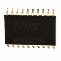
Manufacturer Part Number
BTS711L1
Description
SWITCH 4CHAN HGH SIDE P-DS020-9
Manufacturer
Infineon Technologies
Series
PROFET®r
Type
High Sider
Specifications of BTS711L1
Input Type
Non-Inverting
Number Of Outputs
4
On-state Resistance
165 mOhm
Current - Output / Channel
1.9A
Current - Peak Output
7.5A
Voltage - Supply
5 V ~ 34 V
Operating Temperature
-40°C ~ 150°C
Mounting Type
Surface Mount
Package / Case
DSO-20
Power Load Switch Type
High Side
Input Voltage
34V
On State Resistance
320mohm
Thermal Protection
Yes
On / Enable Input Polarity
Active High
Power Dissipation Pd
3.6W
Current Limit
7.5A
Lead Free Status / RoHS Status
Lead free / RoHS Compliant
Other names
BTS711L1INTR
BTS711L1NT
BTS711L1T
BTS711L1XT
BTS711L1XTINTR
BTS711L1XTINTR
SP000011298
SP000379623
BTS711L1NT
BTS711L1T
BTS711L1XT
BTS711L1XTINTR
BTS711L1XTINTR
SP000011298
SP000379623
Available stocks
Company
Part Number
Manufacturer
Quantity
Price
Company:

Part Number:
BTS711L1
Manufacturer:
FUJITSU
Quantity:
101
Company:
Part Number:
BTS711L1
Manufacturer:
INF
Quantity:
1 340
Part Number:
BTS711L1
Manufacturer:
INFINEON/英飞凌
Quantity:
20 000


Data Sheet
Initial short circuit shutdown time
Parameter and Conditions,
at T
Standby current, all channels off
Leakage output current (included in I
Operating current
Protection Functions
Initial peak short circuit current limit,
Repetitive short circuit current limit,
Output clamp (inductive load switch off)
Thermal overload trip temperature
Thermal hysteresis
Reverse Battery
Reverse battery voltage
Drain-source diode voltage
9
10
11
12
)
diagrams, page 13)
V
I
at V
I
V
) Integrated protection functions are designed to prevent IC destruction under fault conditions described in the
) If channels are connected in parallel, output clamp is usually accomplished by the channel with the lowest
) Requires a 150
(see page 11 and timing diagrams on page 13)
GND
L
(see timing diagrams, page 13)
IN
IN
T
j
= - 1.9 A, T
Add I
data sheet. Fault conditions are considered as "outside" normal operating range. Protection functions are not
designed for continuous repetitive operation.
V
diode has to be limited by the connected load. Note that the power dissipation is higher compared to normal
operating conditions due to the voltage drop across the intrinsic drain-source diode. The temperature
protection is not active during reverse current operation! Input and Status currents have to be limited (see
max. ratings page 3 and circuit page 8).
= 25 °C, V
j
ON(CL)
= 0
= 0
= T
ON(CL)
= I
ST
GND1/2
jt
, if I
= V
bb
ST
j
+ I
bb
= +150°C
= 12 V unless otherwise specified
> 0
- V
GND3/4
9)
resistor in GND connection. The reverse load current through the intrinsic drain-source
, V
OUT
IN
,
10)
= 5V, T
each channel, T
12
)
(V
four parallel channels
four parallel channels
each of the four channels
two parallel channels
two parallel channels
out
j
> V
=-40...+150°C
four channels on:
one channel on:
bb
T
T
bb(off)
(see timing
each channel
)
j,start
j,start
T
11)
T
j
=+150°C:
T
T
j
)
j
=150°C:
=-40°C:
j
= 25°C:
j
=-40°C:
=25°C:
=25°C
6
:
t
I
I
I
I
I
V
T
- V
- V
off(SC)
Symbol
bb(off)
L(off)
GND
L(SCp)
L(SCr)
jt
T
ON(CL)
bb
ON
four times the current of one channel
jt
Smart High-Side Power Switch
twice the current of one channel
150
min
5.5
4.5
2.5
--
--
--
--
--
--
--
--
--
--
--
--
--
--
Values
610
48
9.5
7.5
4.5
typ
28
44
47
10
29
--
--
--
2
8
4
4
4
Rev 1.2, 2010-03-16
max
60
70
12
12
13
11
32
--
--
BTS711L1
--
--
--
--
--
--
--
3
7
Unit
mA
ms
mV
°C
A
A
A
A
V
K
V
Related parts for BTS711L1
Image
Part Number
Description
Manufacturer
Datasheet
Request
R

Part Number:
Description:
Manufacturer:
Infineon Technologies AG
Datasheet:
Part Number:
Description:
Manufacturer:
Infineon Technologies AG
Datasheet:
Part Number:
Description:
Manufacturer:
Infineon Technologies AG
Datasheet:
Part Number:
Description:
Manufacturer:
Infineon Technologies AG
Datasheet:
Part Number:
Description:
Manufacturer:
Infineon Technologies AG
Datasheet:
Part Number:
Description:
Manufacturer:
Infineon Technologies AG
Datasheet:
Part Number:
Description:
Manufacturer:
Infineon Technologies AG
Datasheet:
Part Number:
Description:
16-bit microcontroller with 2x2 KByte RAM
Manufacturer:
Infineon Technologies AG
Datasheet:
Part Number:
Description:
NPN silicon RF transistor
Manufacturer:
Infineon Technologies AG
Datasheet:
Part Number:
Description:
NPN silicon RF transistor
Manufacturer:
Infineon Technologies AG
Datasheet:
Part Number:
Description:
NPN silicon RF transistor
Manufacturer:
Infineon Technologies AG
Datasheet:
Part Number:
Description:
NPN silicon RF transistor
Manufacturer:
Infineon Technologies AG
Datasheet:
Part Number:
Description:
Si-MMIC-amplifier in SIEGET 25-technologie
Manufacturer:
Infineon Technologies AG
Datasheet:
Part Number:
Description:
IGBT Power Module
Manufacturer:
Infineon Technologies AG
Datasheet:
Part Number:
Description:
IC for switching-mode power supplies
Manufacturer:
Infineon Technologies AG
Datasheet: