BTS5240L Infineon Technologies, BTS5240L Datasheet - Page 4
BTS5240L
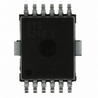
Manufacturer Part Number
BTS5240L
Description
IC SWITCH PWR HISIDE DSO-12
Manufacturer
Infineon Technologies
Type
High Sider
Datasheet
1.BTS5240L.pdf
(17 pages)
Specifications of BTS5240L
Input Type
Non-Inverting
Number Of Outputs
2
On-state Resistance
21 mOhm
Current - Output / Channel
6A
Current - Peak Output
11A
Voltage - Supply
4.5 V ~ 28 V
Operating Temperature
-40°C ~ 150°C
Mounting Type
Surface Mount
Package / Case
DSO-12
Lead Free Status / RoHS Status
Contains lead / RoHS non-compliant
Other names
BTS5240L
BTS5240LINTR
BTS5240LNT
BTS5240LT
SP000014002
BTS5240LINTR
BTS5240LNT
BTS5240LT
SP000014002
Available stocks
Company
Part Number
Manufacturer
Quantity
Price
Company:

Part Number:
BTS5240L
Manufacturer:
INFINEON
Quantity:
3 333
Company:
Part Number:
BTS5240L
Manufacturer:
INFINEON
Quantity:
23 805
Part Number:
BTS5240L
Manufacturer:
INFINEON/英飞凌
Quantity:
20 000


Maximum Ratings at T
Parameter
Supply voltage (overvoltage protection see page 6)
Supply voltage for full short circuit protection; T
Maximum voltage across DMOS
Load dump protection
In = low or high; t
R
R
Load current (Short - circuit current, see page 7)
Operating temperature range
Storage temperature range
Dynamical temperature rise at switching
Power dissipation
Maximal switchable inductance, single pulse
V
I
I
Electrostatic discharge voltage
(Human Body Model)
according to ANSI EOS/ESD - S5.1 - 1993 , ESD STM5.1 - 1998
Continuous input voltage
Voltage at current limit adjustment pin
Current through current limit adjustment pin
Current through input pin (DC)
Current through sense (DC)
1 18...28 V for 100 hours
2 only single pulse, R
line, contact and generator impedances.
3 Supply voltage higher than V
4 R
5 Current limit is a protection function. Operation in current limitation is considered as "outside" normal operating
range. Protection functions are not designed for continuous repetitive operation.
6 Device on 50mm*50mm*1.5mm epoxy PCB FR4 with 6 cm2 (one layer, 70µm thick) copper area for V
connection. PCB is vertical without blown air.
L
L
bb
L
L
= 6 A, E
= 12 A, E
I = internal resistance of the load dump test pulse generator.
= 2.25
= 6.8
=12V, T
AS
jstart
AS
= 0.319 J, R
= 0.679 J, R
=150°C;
d
6)
L = 200 m
= 400 ms; R
(DC), one channel active
3)
j
=25°C, unless otherwise specified
V
bb(AZ) require an external current limit for the GND(150 resistor) and sense pin.
LoadDump
L
L
= 0
= 0
; L = 8 µH ; R and L are describing the complete circuit impedance including
(see page 11)
I
4)
(see diagrams on page 12)
,
= 2
,
= V
A
two parallel channels:
+ V
Page 4
S
; V
j
A
T
= -40...150°C V
one channel:
A
= 13,5 V
= 85 °C
OUT:
IS:
IN:
Symbol
V
V
V
I
T
T
dT
P
Z
V
V
V
I
I
I
L
CLA
IN
IS
j
stg
L(s)
bb
bb(SC)
ON
Loaddump
tot
ESD
IN
CLA
-40...+150 °C
-55...+150
-10...16
-5...+10
I
-10...16
L(lim)
Value
28
28
BTS 5240L
2005-06-03
1,4
9.8
5.2
1.0
2.0
4.0
52
40
53
60
5.0
5.0
1)
2)
5)
bb
Unit
V
A
K
W
mH
kV
V
mA
Related parts for BTS5240L
Image
Part Number
Description
Manufacturer
Datasheet
Request
R

Part Number:
Description:
Manufacturer:
Infineon Technologies AG
Datasheet:
Part Number:
Description:
Manufacturer:
Infineon Technologies AG
Datasheet:
Part Number:
Description:
Manufacturer:
Infineon Technologies AG
Datasheet:
Part Number:
Description:
Manufacturer:
Infineon Technologies AG
Datasheet:
Part Number:
Description:
Manufacturer:
Infineon Technologies AG
Datasheet:
Part Number:
Description:
Manufacturer:
Infineon Technologies AG
Datasheet:
Part Number:
Description:
Manufacturer:
Infineon Technologies AG
Datasheet:
Part Number:
Description:
16-bit microcontroller with 2x2 KByte RAM
Manufacturer:
Infineon Technologies AG
Datasheet:
Part Number:
Description:
NPN silicon RF transistor
Manufacturer:
Infineon Technologies AG
Datasheet:
Part Number:
Description:
NPN silicon RF transistor
Manufacturer:
Infineon Technologies AG
Datasheet:
Part Number:
Description:
NPN silicon RF transistor
Manufacturer:
Infineon Technologies AG
Datasheet:
Part Number:
Description:
NPN silicon RF transistor
Manufacturer:
Infineon Technologies AG
Datasheet:
Part Number:
Description:
Si-MMIC-amplifier in SIEGET 25-technologie
Manufacturer:
Infineon Technologies AG
Datasheet:
Part Number:
Description:
IGBT Power Module
Manufacturer:
Infineon Technologies AG
Datasheet:
Part Number:
Description:
IC for switching-mode power supplies
Manufacturer:
Infineon Technologies AG
Datasheet: