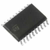
TDE1897RFP STMicroelectronics, TDE1897RFP Datasheet - Page 5

TDE1897RFP
Manufacturer Part Number
TDE1897RFP
Description
IC SWITCH .5A INTEL PWR 20 SOIC
Manufacturer
STMicroelectronics
Type
High Sider
Datasheet
1.TDE1897RFPT.pdf
(12 pages)
Specifications of TDE1897RFP
Input Type
Differential
Number Of Outputs
1
Current - Output / Channel
500mA
Current - Peak Output
1.5A
Voltage - Supply
18 V ~ 35 V
Operating Temperature
-25°C ~ 85°C
Mounting Type
Surface Mount
Package / Case
20-SOIC (7.5mm Width)
Lead Free Status / RoHS Status
Lead free / RoHS Compliant
On-state Resistance
-
Other names
497-2186-5
Available stocks
Company
Part Number
Manufacturer
Quantity
Price
APPLICATION INFORMATION
DEMAGNETIZATION OF INDUCTIVE LOADS
An internal zener diode, limiting the voltage
across the Power MOS to between 45 and 55V
(V
inductive loads without external clamping devices.
The maximum energy that can be absorbed from
an inductive load is specified as 200mJ (at
T
To define the maximum switching frequency three
points have to be considered:
1) The total power dissipation is the sum of the
2) The total energy W dissipated in the device
3) In normal conditions the operating Junction
Figure 2: Inductive Load Equivalent Circuit
j
cl
= 85 C).
), provides safe and fast demagnetization of
On State Power and of the Demagnetization
Energy multiplied by the frequency.
during a demagnetization cycle (figg. 2, 3) is:
W
Where:
temperature should remain below 125 C.
V
L = inductive load;
R
Vs = supply voltage;
I
O
cl
L
= I
V
= resistive load;
= clamp voltage;
cl
LOAD
R
L
L
I
o
–
V
cl
R
– V
L
s
log 1
V
cl
V
– V
s
s
Figure 3: Demagnetization Cycle Waveforms
Figure 4: Normalized R
1.8
1.6
1.4
1.2
1.0
0.8
0.6
-25
Temperature
0
=
RDSON (Tj=25˚C)
25
RDSON (Tj)
TDE1897R - TDE1898R
50
DSON
75
vs. Junction
100
125
D93IN018
Tj (˚C)
5/12


