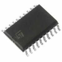
TDE1897RFP STMicroelectronics, TDE1897RFP Datasheet - Page 6

TDE1897RFP
Manufacturer Part Number
TDE1897RFP
Description
IC SWITCH .5A INTEL PWR 20 SOIC
Manufacturer
STMicroelectronics
Type
High Sider
Datasheet
1.TDE1897RFPT.pdf
(12 pages)
Specifications of TDE1897RFP
Input Type
Differential
Number Of Outputs
1
Current - Output / Channel
500mA
Current - Peak Output
1.5A
Voltage - Supply
18 V ~ 35 V
Operating Temperature
-25°C ~ 85°C
Mounting Type
Surface Mount
Package / Case
20-SOIC (7.5mm Width)
Lead Free Status / RoHS Status
Lead free / RoHS Compliant
On-state Resistance
-
Other names
497-2186-5
Available stocks
Company
Part Number
Manufacturer
Quantity
Price
TDE1897R - TDE1898R
WORST CONDITION POWER DISSIPATION IN
THE ON-STATE
In IPS applications the maximum average power
dissipation occurs when the device stays for a
long time in the ON state. In such a situation the
internal temperature depends on delivered cur-
rent (and related power), thermal characteristics
of the package and ambient temperature.
At ambient temperature close to upper limit
(+85°C) and in the worst operating conditions, it is
possible that the chip temperature could increase
so much to make the thermal shutdown proce-
dure untimely intervene.
Our aim is to find the maximum current the IPS
can withstand in the ON state without thermal
shutdown intervention, related to ambient tem-
perature. To this end, we should consider the fol-
lowing points:
1) The ON resistance R
2)
6/12
a) power lost in the switch:
b) power due to quiescent current in the ON
c) an external LED could be used to visualize
where:
NDMOS (the real switch) of the device in-
creases with its temperature.
Experimental results show that silicon resistiv-
ity increases with temperature at a constant
rate, rising of 60% from 25°C to 125°C.
The relationship between R
perature is therefore:
device is due to three contributes:
Thus the total ON state power consumption is
given by:
In the right side of equation 1, the second and
In the ON state the power dissipated in the
P
rent);
state Iq, sunk by the device in addition to
I
the switch state (OUTPUT STATUS pin).
Such a LED is driven by an internal current
source (delivering I
the voltage drop across the LED, the dissi-
pated power is: P
out
T
R
k is the constant rate (k
(see fig. 4).
P
out
j
DSON0
: P
R
is the silicon temperature in °C
on
DSON
q
I
out
P
is R
I
out
q
2
R
DSON
V
R
DSON0
P
s
DSON
(V
q
os
at T
os
s
) and therefore, if V
is the supply voltage);
P
(I
j
I
1
=25°C
out
os
DSON
os
is the output cur-
k
4.711
V
DSON
of the output
T
s
j
V
25
10
and tem-
(1)
os
3
.
)
os
is
3) The chip temperature must not exceed
Referring to application circuit in fig. 5, let us con-
sider the worst case:
- The supply voltage is at maximum value of in-
the third element are constant, while the first
one increases with temperature because
R
in order do not lose the control of the device.
The heat dissipation path is represented by
the thermal resistance of the system device-
board-ambient (R
tions, this parameter relates the power dissi-
pated P
the ambient temperature T
From this relationship, the maximum power P
which can be dissipated without exceeding
Replacing the expression (1) in this equation
and solving for I
current versus ambient temperature relation-
ship:
where R
course, I
maximum operative current I
nominal).
From the expression (2) we can also find the
maximum ambient temperature T
a given power P
In particular, this relation is useful to find the
maximum ambient temperature T
which I
dustrial bus (30V instead of the 24V nominal
value). This means also that I
T
DSON
Lim at a given ambient temperature T
I
T
Lim
outx
ambx
j
P
q
T
outx
increases as well.
T
on
amb
amb
outx
DSON
I
P
out
can be delivered:
P
to the silicon temperature T
Lim
os
on
2
values are top limited by the
P
x is R
Lim
on
out
R
on
Lim P
R
th
, we can find the maximum
can be dissipated:
DSONx
I
th
Lim T
R
). In steady state condi-
outx
R
th
R
T
DSON
th
R
2
amb
th
on
DSONx
amb
R
P
amb
R th
DSONx
at T
q
outx
:
P
q
P
outx
rises of 25%
amb
j
= Lim. Of
os
P
(4)
(2)
at which
ambx
amb
os
(500mA
R
j
is:
th
and
Lim
on
at


