MC33289DWR2 Freescale Semiconductor, MC33289DWR2 Datasheet - Page 2
MC33289DWR2
Manufacturer Part Number
MC33289DWR2
Description
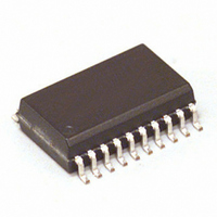
IC SWITCH DUAL H-SIDE 20-SOIC
Manufacturer
Freescale Semiconductor
Type
High Sider
Datasheet
1.MC33289DW.pdf
(11 pages)
Specifications of MC33289DWR2
Input Type
Non-Inverting
Number Of Outputs
2
On-state Resistance
40 mOhm
Current - Peak Output
9A
Voltage - Supply
6 V ~ 27 V
Operating Temperature
-40°C ~ 125°C
Mounting Type
Surface Mount
Package / Case
20-SOIC (7.5mm Width)
Lead Free Status / RoHS Status
Contains lead / RoHS non-compliant
Current - Output / Channel
-
Other names
MC33289DWR2TR
Available stocks
Company
Part Number
Manufacturer
Quantity
Price

Part Number:
MC33289DWR2
Manufacturer:
FREESCALE
Quantity:
20 000
Company:
Part Number:
MC33289DWR2G
Manufacturer:
MPS
Quantity:
3 000


Table 1. Pin Function Description
2
33289
PIN CONNECTIONS
1, 2, 5, 6, 15, 16,
Pin Number
3, 4, 18, 17
19, 20
8, 13
9, 12
10
11
Pin Name
OUT1
OUT2
OLDE
GND
VBAT
ST1
ST2
IN1
IN2
Supply Voltage
OUTPUT Channel 1
OUTPUT Channel 2
INPUT Channel 1
INPUT Channel 2
Status for Channel 1
Status for Channel 2
Open Load Detection
Enable
GROUND
Pin Function
Figure 2. 33289 Pin Connections
VBAT
VBAT
OUT1
OUT1
VBAT
VBAT
NC
IN1
ST1
OLDE
PIN CONNECTIONS
These are the power supply pins of the device. These pins are directly connected
with the lead frame of the package and are tied to the drain of the switching
MOSFET. These pins can be directly connected to the battery voltage. In addition
to their supply function, these pins participate to the thermal behavior of the
device in conducting the heat from the switching MOSFET to the printed circuit
board.
Pins 3 and 4 are the output 1 pins. Pins 17 and 18 are the output 2 pins. They are
directly connected to the source of the power MOSFET. These pins are used by
the control circuitry to sense the device output voltage. The R
per output at 25°C and will increase to a maximum of 75 mΩ at 150°C junction
temperature.
These are the device input pins which directly control their associated outputs.
The levels are CMOS compatible. When the input is a logic low, the associated
output MOSFET is in the off state. When input is high, the MOSFET is turned on
and the load is activated.
When both inputs are low, the device is in standby mode and its supply current is
reduced. Each input pin has an internal active pull down, so that it will not float if
disconnected.
These pins are the channel 1 and channel 2 fault detection flags. Their internal
structure is an open drain architecture with an internal clamp at 6.0 V. An external
pull up resistor connected to V
If the device is in its normal condition the status lines will be high. If open load or
other fault occurs, the associated channel status flag will be pulled low. See
Functional Truth Table.
This pin is a digital input which enables the open load current diagnostic circuitry.
When OLDE is a logic low, the open load circuitry is not powered and the device’s
bias current draw is at a minimum. If OLDE is a logic high, the open load circuitry
is functional at the price of a higher bias current draw. OLDE pin has a pull down
resistor.
This is the GND pin of the device.
10
1
2
3
4
5
6
7
8
9
PIN ASSIGNMENT
11
15
13
20
19
18
17
16
14
12
VBAT
VBAT
OUT2
OUT2
VBAT
VBAT
NC
IN2
ST2
GND
DD
(5.0 V) is needed. This is an active low output.
Definition
Analog Integrated Circuit Device Data
Freescale Semiconductor
DSON
is 40 mΩ max
Related parts for MC33289DWR2
Image
Part Number
Description
Manufacturer
Datasheet
Request
R


Part Number:
Description:
Manufacturer:
Freescale Semiconductor, Inc
Datasheet:
Part Number:
Description:
Manufacturer:
Freescale Semiconductor, Inc
Datasheet:
Part Number:
Description:
Manufacturer:
Freescale Semiconductor, Inc
Datasheet:
Part Number:
Description:
Manufacturer:
Freescale Semiconductor, Inc
Datasheet:
Part Number:
Description:
Manufacturer:
Freescale Semiconductor, Inc
Datasheet:
Part Number:
Description:
Manufacturer:
Freescale Semiconductor, Inc
Datasheet:
Part Number:
Description:
Manufacturer:
Freescale Semiconductor, Inc
Datasheet:
Part Number:
Description:
Manufacturer:
Freescale Semiconductor, Inc
Datasheet:
Part Number:
Description:
Manufacturer:
Freescale Semiconductor, Inc
Datasheet:
Part Number:
Description:
Manufacturer:
Freescale Semiconductor, Inc
Datasheet:
Part Number:
Description:
Manufacturer:
Freescale Semiconductor, Inc
Datasheet:
Part Number:
Description:
Manufacturer:
Freescale Semiconductor, Inc
Datasheet:
Part Number:
Description:
Manufacturer:
Freescale Semiconductor, Inc
Datasheet:
Part Number:
Description:
Manufacturer:
Freescale Semiconductor, Inc
Datasheet: