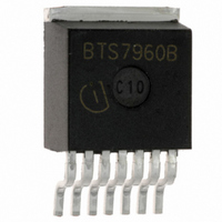
BTS7960B Infineon Technologies, BTS7960B Datasheet
BTS7960B
Specifications of BTS7960B
BTS7960BT
BTS7960BT
SP000014711
Available stocks


Related parts for BTS7960B

BTS7960B Summary of contents
Page 1
et . ber ...
Page 2
Product Summary . . . . . . . . . . . . . . . . . . . . . . . . . . . . . . . . . . . . . . ...
Page 3
High Current PN Half Bridge TM NovalithIC Product Summary The BTS 7960 is a fully integrated high current half bridge for motor drive applications part of the TM NovalithIC family containing one p-channel highside MOSFET and one n-channel ...
Page 4
Overview The BTS 7960 is part of the NovalithIC family containing three separate chips in one package: One p-channel highside MOSFET and one n-channel lowside MOSFET together with a driver IC, forming a fully integrated high current half-bridge. All ...
Page 5
Terms Following figure shows the terms used in this data sheet Figure 2 Terms Data Sheet I ...
Page 6
Pin Configuration 2.1 Pin Assignment BTS 7960B P-TO-263 Figure 3 Pin Assignment BTS 7960B and BTS 7960P (top view) 2.2 Pin Definitions and Functions Pin Symbol 1 GND ...
Page 7
Maximum Ratings T -40 C < < 150 C (unless otherwise specified) j Pos Parameter Electrical Maximum Ratings 3.0.1 Supply voltage 3.0.2 Logic Input Voltage 3.0.3 HS/LS continuous drain current 3.0.4 HS pulsed drain current 3.0.5 LS pulsed drain ...
Page 8
Block Description and Characteristics 4.1 Supply Characteristics T – < < 150 < j Pos. Parameter General 4.1.1 Operating Voltage 4.1.2 Supply Current 4.1.3 Quiescent Current Data Sheet High Current PN Half Bridge Block ...
Page 9
Power Stages The power stages of the BTS 7960 consist of a p-channel vertical DMOS transistor for the high side switch and a n-channel vertical DMOS transistor for the low side switch. All protection and diagnostic functions are located ...
Page 10
Power Stages - Static Characteristics T – < < 150 < j Pos. Parameter High Side Switch - Static Characteristics 4.2.1 On state high side resistance 4.2.2 Leakage current high side 4.2.3 Reverse diode ...
Page 11
Switching Times dr(HS) r(HS) V OUT 90% 10% Figure 5 Definition of switching times high side ( (LS) f (LS) V OUT 90% 10% Figure 6 Definition of switching times low side ...
Page 12
Power Stages - Dynamic Characteristics T V -40 C < < 150 Pos. Parameter HIgh Side Switch Dynamic Characteristics 4.2.7 Rise-time of HS 4.2.8 Slew rate HS on 4.2.9 Switch on delay ...
Page 13
T V -40 C < < 150 Pos. Parameter Low Side Switch Dynamic Characteristics 4.2.13 Rise-time of LS 4.2.14 Slew rate LS switch off 4.2.15 Switch off delay time LS 4.2.16 Fall-time of ...
Page 14
Protection Functions The device provides integrated protection functions. These are designed to prevent IC destruction under fault conditions described in the data sheet. Fault conditions are considered as “outside” normal operating range. Protection functions are not to be used ...
Page 15
IN pin are ignored. However, the INH pin can still be used to switch both MOSFETs off. t After the switches return to their initial setting. The error signal at the IS pin is reset CLS t after 2 * ...
Page 16
High Side Switch -40° 25° 150° CLH Figure 9 Typical Current Limitation Detection Levels vs. Supply Voltage ...
Page 17
Electrical Characteristics - Protection Functions T – < < 150 < j Pos. Parameter Under Voltage Shut Down 4.3.1 Switch-ON voltage 4.3.2 Switch-OFF voltage 4.3.3 ON/OFF hysteresis Over Voltage Lock Out 4.3.4 Switch-ON voltage ...
Page 18
Control and Diagnostics 4.4.1 Input Circuit The control inputs IN and INH consist of TTL/CMOS compatible schmitt triggers with hysteresis which control the integrated gate drivers for the MOSFETs. Setting the INH pin to high enables the device. In ...
Page 19
Normal operation: current sense mode VS ESD- Load Sense output I logic IS(lim) Figure 10 Sense current and fault current Data Sheet High Current PN Half Bridge Block Description and Characteristics Fault condition: error flag mode ...
Page 20
Truth Table Device State Normal operation Over-voltage (OV) Under-voltage (UV) Overtemperature or short circuit of HSS or LSS Current limitation mode 1 Inputs: Switches 0 = Logic LOW OFF = switched off 1 = Logic HIGH ON = switched ...
Page 21
Electrical Characteristics - Control and Diagnostics T – < < 150 < j Pos. Parameter Control Inputs (IN and INH) 4.4.1 High level voltage INH, IN 4.4.2 Low level voltage INH, IN 4.4.3 Input ...
Page 22
Thermal Characteristics Pos Parameter 5.0.1 Thermal Resistance Junction-Case, Low Side Switch thjc(LS) j(LS) 5.0.2 Thermal Resistance Junction-Case, High Side Switch thjc(HS) j(HS) 5.0.3 Thermal Resistance Junction-Case, both Switches R T ...
Page 23
Application 6.1 Application Example Microcontroller µC Reset Vdd Vss I/O I/O I/O I/O BTS 7960B INH Figure 11 Application Example: H-Bridge with two BTS 7960B 6.2 Layout Considerations Due to the fast switching times for high ...
Page 24
Package Outlines P-TO-263-7 P-TO-263-7 (Plastic Transistor Single Outline Package) 0...0. 0 1.27 1) Shear and punch direction no burrs this surface Back side, heatsink contour All metal sufaces tin plated, except area of cut . ...
Page 25
Package Outlines P-TO-220-7 P-TO-220-7 (Plastic Transistor Single Outline Package) C 0...0. 0 1.27 0. Shear and punch direction no burrs this surface Back side, heatsink contour All m etal surfaces tin plated, except ...
Page 26
Revision History Revision Date n.a. 2004-03-18 0.9 2004-10-10 1.0 2004-11-30 1.1 2004-12-07 Data Sheet Changes / Comments Target Data Sheet Target Data Sheet converted to new layout Preliminary Data Sheet “Preliminary” removed; No other changes 25 High Current PN ...
Page 27
... Infineon Technologies Office. Infineon Technologies Components may only be used in life-support devices or systems with the express written approval of Infineon Technologies failure of such components can reasonably be expected to cause the failure of that life-support device or system affect the safety or effectiveness of that device or system. Life support devices or systems are intended to be implanted in the human body support and/or maintain and sustain and/or protect human life ...
Page 28
... Published by Infineon Technologies AG ...