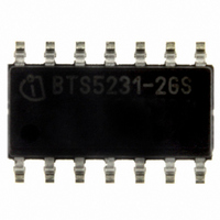
BTS5231-2GS Infineon Technologies, BTS5231-2GS Datasheet - Page 11

BTS5231-2GS
Manufacturer Part Number
BTS5231-2GS
Description
IC PWR SWITCH HISIDE PGDSO-14-31
Manufacturer
Infineon Technologies
Series
PROFET®r
Type
High Sider
Datasheet
1.BTS5231-2GS.pdf
(27 pages)
Specifications of BTS5231-2GS
Package / Case
DSO-14
Input Type
Non-Inverting
Number Of Outputs
2
On-state Resistance
140 mOhm
Current - Output / Channel
1.8A
Current - Peak Output
10A
Voltage - Supply
4.5 V ~ 28 V
Operating Temperature
-40°C ~ 150°C
Mounting Type
Surface Mount
On Resistance (max)
140 mOhms
Maximum Operating Temperature
+ 150 C
Minimum Operating Temperature
- 40 C
Maximum Power Dissipation
900 mW
Mounting Style
SMD/SMT
Supply Current
3.8 mA
Power Load Switch Type
High Side
Input Voltage
28V
Current Limit
8A
On State Resistance
0.14ohm
Thermal Protection
ESD
Power Dissipation Pd
900mW
No. Of Outputs
2
Internal Switch
No
Rohs Compliant
Yes
Distribution Switch Case Style
SOIC
Lead Free Status / RoHS Status
Lead free / RoHS Compliant
Lead Free Status / RoHS Status
Lead free / RoHS Compliant, Lead free / RoHS Compliant
Other names
BTS5231-2GSINTR
BTS52312GSXT
SP000281794
BTS52312GSXT
SP000281794
Available stocks
Company
Part Number
Manufacturer
Quantity
Price
Part Number:
BTS5231-2GS
Manufacturer:
INFINEON/英飞凌
Quantity:
20 000
A high signal at the input pin causes the power DMOS to switch on with a dedicated
slope, which is optimized in terms of EMC emission.
Figure 6
4.1.3
When switching off inductive loads with high-side switches, the voltage
ground potential, because the inductance intends to continue driving the current.
Figure 7
To prevent destruction of the device, there is a voltage clamp mechanism implemented
that keeps that negative output voltage at a certain level (
Figure 8
Data Sheet
for details. Nevertheless, the maximum allowed load inductance is limited.
Inductive Output Clamp
Switching a Load (resistive)
Output Clamp (OUT1 and OUT2)
V
90%
70%
30%
10%
OUT
IN
t
ON
V
bb
dV /dt
ON
Block Description and Electrical Characteristics
11
GND
VBB
Smart High-Side Power Switch
OUT
dV /dt
70%
30%
ON
V
OUT
V
I
t
OFF
L
OUT(CL)
L,
R
L
t
t
). See
V
BTS5231-2GS
OUT
V1.1, 2007-06-14
Figure 7
drops below
OutputClamp .em
SwitchOn.emf
and


