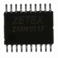
ZXBM1017ST20TC Diodes Zetex, ZXBM1017ST20TC Datasheet - Page 2

ZXBM1017ST20TC
Manufacturer Part Number
ZXBM1017ST20TC
Description
IC MOTOR CTRLR 1PH BLDC 20-TSSOP
Manufacturer
Diodes Zetex
Datasheet
1.ZXBM1017ST20TC.pdf
(10 pages)
Specifications of ZXBM1017ST20TC
Applications
DC Motor Controller, Brushless (BLDC)
Number Of Outputs
1
Voltage - Supply
6.7 V ~ 18 V
Operating Temperature
-40°C ~ 110°C
Mounting Type
Surface Mount
Package / Case
20-TSSOP
Lead Free Status / RoHS Status
Lead free / RoHS Compliant
Current - Output
-
Voltage - Load
-
Other names
ZXBM1017ST20TR
Available stocks
Company
Part Number
Manufacturer
Quantity
Price
Company:
Part Number:
ZXBM1017ST20TC
Manufacturer:
Diodes/Zetex
Quantity:
5 000
Part Number:
ZXBM1017ST20TC
Manufacturer:
ZETEX
Quantity:
20 000
1) Maximum allowable Power Dissipation, P
2) Power consumed by the device, PT, can be
P
where
and
and
Absolute Maximum Ratings
ZXBM1017
Parameter
Supply Voltage
Input Current
Maximum Input Voltage
Maximum Output Voltage
Power Dissipation
Operating Temp.
Storage Temp.
T
= P
shown plotted against Ambient Temperature,T
in the accompanying Power Derating Curve,
indicating the Safe Operating Area for the device.
calculated from the equation:
Q
+ P
where IOH is the maximum application
Ph1Lo and Ph2Lo output currents
P
current conditions, given by:
P
where Vcc is the maximum application
device Supply Voltage
and Icc is the maximum Supply Current
given in the Electrical Characteristics
P
of the phase outputs Ph1Hi or Ph2Hi being
active, given by:
P
where I
Ph1Hi and Ph2Hi output currents
and V
Voltage for the Ph1Hi and Ph2Hi outputs
given in the Electrical Characteristics
P
of the phase outputs Ph1Lo or Ph2Lo being
active, given by:
P
Q i
Q
PhHi
PhHi
PhLo
PhLo
PhHi
= V
s power dissipated under quiescent
OL
is power generated due to either one
= I
+ P
is power generated due to either one
CC
= I
OL
is the maximum Low Level Output
OL
OH
PhLo
x I
is the maximum application
x V
CC
x (V
+ P
OL
CC
TR
- V
+ P
OH
Symbol
V CCmax
I CCmax
V Imax
V Omax
P Dmax
T OPR
T STG
HB
)
+ P
FGRD
D
, is
A
,
2
and
and
and
Limits
-0.6 to 20
200
-0.6 to Vcc+0.5
-0.6 to Vcc+0.5
800
-40 to 110
-55 to 150
and V
Supply Voltage
and V
Voltage for the Ph1Lo and Ph2Lo outputs
given in the Electrical Characteristics.
P
Reference source current, given by:
P
where I
ThRef output current
and V
Supply Voltage
and V
voltage
P
source current, given by:
P
where I
Bias output current
and V
P
both the Frequency Generator and Locked
Rotor Detect outputs being active, given by:
P
where I
or RD output current
and V
Voltage
TR
TR
HB
HB
FGRD
FGRD
is power generated due to the Network
= I
is power generated due to the Hall Bias
= I
CC
CC
ThRef
HB
OH
OL
HB
is power generated due to either or
HB
= I
OThRef
OThRef
OL
is the maximum application device
is the maximum application device
is the Hall Bias voltage
is the minimum High Level Output
is the FG or RD Low Level Output
OL
x (V
is the maximum application Hall
is the maximum application FG
is the Network Reference
x V
CC
x (V
is the maximum application
OL
- V
Unit
V
mA
V
V
mW
°C
°C
CC
HB
- V
ISSUE 4 - MAY 2007
)
ThRef
)


