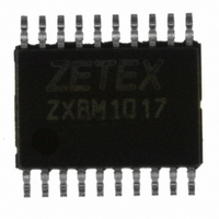
ZXBM1017ST20TC Diodes Zetex, ZXBM1017ST20TC Datasheet - Page 6

ZXBM1017ST20TC
Manufacturer Part Number
ZXBM1017ST20TC
Description
IC MOTOR CTRLR 1PH BLDC 20-TSSOP
Manufacturer
Diodes Zetex
Datasheet
1.ZXBM1017ST20TC.pdf
(10 pages)
Specifications of ZXBM1017ST20TC
Applications
DC Motor Controller, Brushless (BLDC)
Number Of Outputs
1
Voltage - Supply
6.7 V ~ 18 V
Operating Temperature
-40°C ~ 110°C
Mounting Type
Surface Mount
Package / Case
20-TSSOP
Lead Free Status / RoHS Status
Lead free / RoHS Compliant
Current - Output
-
Voltage - Load
-
Other names
ZXBM1017ST20TR
Available stocks
Company
Part Number
Manufacturer
Quantity
Price
Company:
Part Number:
ZXBM1017ST20TC
Manufacturer:
Diodes/Zetex
Quantity:
5 000
Part Number:
ZXBM1017ST20TC
Manufacturer:
ZETEX
Quantity:
20 000
PIN FUNCTIONAL DESCRIPTION
H+ - Positive Hall input
H- - Negative Hall input
The rotor position is detected by a Hall sensor, with the
output applied to the H+ and H- pins. This sensor can be
either a 4 pin 'naked' Hall device or of the 3 pin buffered
switching type. For a 4 pin device the differential Hall
output signal is connected to the H+ and H- pins. For a
buffered Hall sensor the Hall device output is attached
to the H+ pin, with a pull-up attached if needed, whilst
the H- pin has an external potential divider attached to
hold the pin at half Vcc. When H+ is high in relation to
H-, Ph2 is the active drive.
H-Bias- Hall Bias Output
This is a 1.75V nominal voltage source to bias a differential
unbufferred Hall sensor when that type is used.
ThRef - Network Reference
This is a reference voltage of nominal 5V and is used by
external networks to set up the SPD and SMIN pins
control voltages.
It is designed for the ability to 'source' current and
therefore it will not 'sink' any current from a higher
voltage. The current drawn from the pin by the
minimum speed potential divider to pin SMIN and any
voltage setting network on the SPD pin should not
exceed 10mA in total.
SPD - Speed Control Input
The voltage applied to the SPD pin provides control
over the Fan Motor speed by varying the Pulse Width
Modulated (PWM) drive ratio at the Ph1Lo and Ph2Lo
outputs. The control signal takes the form of a voltage
input of range 3V to 1V, representing 0% to 100% drive
respectively.
If variable speed control is not required this pin can be
left with an external potential divider to set a fixed
speed or tied to ground to provide full speed i.e. 100%
PWM drive.
The advantage of a fixed potential divider is so that the
benefit of the current control can be achieved.
If required this pin can also be used as a disable pin.
The application of a voltage >3.0V will force the PWM
drive fully off, in effect disabling the drive.
SMIN - Sets Minimum Speed
A voltage can be set on this pin via a potential divider
between the ThRef and Gnd. This voltage is monitored
by the SPD pin such that the SPD voltage cannot rise
above the SMIN Voltage. As a higher voltage on the
ZXBM1017
6
SPD pin represents a lower speed it therefore restricts
the lower speed range of the fan. If this feature is not
required the pin is left tied to ThRef so no minimum
speed will be set.
If the fan is being controlled from an external voltage
source either this feature should not be used or if it is
required then a >1k resistor should be placed in series
with the SPD pin.
ComDel - Adjusts the Commutation Delay
The ZXBM1017 has a fixed internal commutation delay
of 100us, however, there may be cases where this
needs to be adjusted to a different value. A resistor can
be attached to this pin to enable the delay to be
lengthened or shortened dependant upon application.
A resistor applied between the ComDel pin and Gnd
will lengthen the delay and a resistor applied between
the ComDel pin and ThRef will shorthen the delay. The
following Table indicates the delay expected for a
given resistor value.
Typical Commutation Delay
CPWM - Sets PWM Frequency
This pin has an external capacitor attached to set the
PWM frequency for the Phase drive outputs. A
capacitor value of 0.1nF will provide a PWM frequency
of typically 24kHz.
The C
following equation:
Where:
Resistor to
PWM
100k
220k
ThRef
t
PWM
-
-
-
=
timing period (t
V
threshold voltages
I
discharge currents in A.
t
C = C
(
PWMC
PWM
V
THH
THH
I
PWM
−
PWMC
and V
is in s
Resistor to Gnd
V
and I
THL
)
+15, in pF
xC
470k
300k
THL
PWMD
-
-
-
PWM
+
are the C
(
V
THH
are the charge and
) is determined by the
I
ISSUE 4 - MAY 2007
−
PWMD
V
THL
PWM
)
Delay ( s)
xC
pin
120
168
28
40
80


