LT3572EUF#PBF Linear Technology, LT3572EUF#PBF Datasheet - Page 5
LT3572EUF#PBF
Manufacturer Part Number
LT3572EUF#PBF
Description
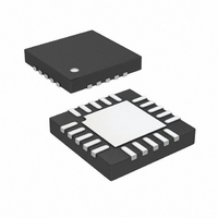
IC DRIVER PIEZO DUAL 20-QFN
Manufacturer
Linear Technology
Datasheet
1.LT3572EUFPBF.pdf
(12 pages)
Specifications of LT3572EUF#PBF
Applications
Piezo Motor Driver
Number Of Outputs
2
Voltage - Load
5 V ~ 40 V
Voltage - Supply
2.7 V ~ 10 V
Operating Temperature
-40°C ~ 85°C
Mounting Type
Surface Mount
Package / Case
20-QFN
Lead Free Status / RoHS Status
Lead free / RoHS Compliant
Current - Output
-
Available stocks
Company
Part Number
Manufacturer
Quantity
Price


PIN FUNCTIONS
SW (Pin 1): Switch Node. This pin connects to the col-
lector of an internal NPN power switch.
V
bypassed with a capacitor.
SYNC (Pin 3): Synchronization Pin. This pin is used to
synchronize the internal oscillator to an external signal.
The synchronizing range is 15% above the free running
frequency set by the RT pin up to 2.5MHz. If not used,
this pin must be tied to GND.
RT (Pin 4): Frequency Set Pin. Place a resistor to GND
to set the internal frequency. The range of oscillation is
500kHz to 2.25MHz.
GND (Pins 5, 9, 20): Ground.
PWMB (Pin 6): Logic Input for the Driver. A high signal
on this input sets OUTB high and OUTB low.
PWMA (Pin 7): Logic Input for the Driver. A high signal
on this input sets OUTA high and OUTA low.
V
Input Supply for the Drivers.
SHDN (Pin 10): Shutdown Pin. Tie to 1.5V or more to
enable the switcher. Pull low to disable the switcher.
SHDNA (Pin 11): Shutdown Pin. Tie to 1.5V or more to
enable OUTA and OUTA. Pull low to place OUTA and OUTA
in a high impedance state.
IN
OUT
(Pin 2): Input Supply Pin. This pin must be locally
(Pin 8): Output for the Switching Regulator and the
SHDNB (Pin 12): Shutdown Pin. Tie to 1.5V or more to
enable OUTB and OUTB. Pull low to place OUTB and OUTB
in a high impedance state.
FB (Pin 13): Feedback Pin. The LT3572 regulates this pin
to 1.225V. Connect the feedback resistors to this pin to
set the output voltage for the switching regulator.
SS (Pin 14): Soft-Start Pin. Place a soft-start capacitor
here. A capacitor on the soft-start pin slowly ramps the
current limit of the part from 0A to 1.3A.
PGOOD (Pin 15): This pin is an open-drain output that
pulls low when the FB pin is within 95% of its regulation
value.
OUTB (Pin 16): The Output Driver. This node switches
between V
OUTB (Pin 17): The Output Driver. This node switches
between V
OUTA (Pin 18): The Output Driver. This node switches
between V
OUTA (Pin 19): The Output Driver. This node switches
between V
Exposed Pad (Pin 21): Ground. The Exposed Pad of the
package provides both electrical contact to ground and
good thermal contact to the printed circuit board. The
Exposed Pad must be soldered to the circuit board for
proper operation.
OUT
OUT
OUT
OUT
and GND and is inverted from OUTB.
and GND.
and GND .
and GND and is inverted from OUTA.
LT3572
3572fa
5
Related parts for LT3572EUF#PBF
Image
Part Number
Description
Manufacturer
Datasheet
Request
R

Part Number:
Description:
CD ROM LINEARVIEW DATASHEETS
Manufacturer:
Linear Technology

Part Number:
Description:
Standalone Linear Li-Ion Battery Charger with Thermal Regulation in ThinSOT
Manufacturer:
Linear Technology Corporation
Datasheet:
Part Number:
Description:
Low noise, high frequency, 8th order linear phase lowpass filter
Manufacturer:
Linear Technology Corporation
Datasheet:
Part Number:
Description:
Manufacturer:
Linear Technology Corporation
Datasheet:
Part Number:
Description:
Manufacturer:
Linear Technology Corporation
Datasheet:
Part Number:
Description:
Manufacturer:
Linear Technology Corporation
Datasheet:
Part Number:
Description:
Manufacturer:
Linear Technology Corporation
Datasheet:
Part Number:
Description:
Manufacturer:
Linear Technology Corporation
Datasheet:
Part Number:
Description:
Manufacturer:
Linear Technology Corporation
Datasheet:
Part Number:
Description:
Manufacturer:
Linear Technology Corporation
Datasheet:
Part Number:
Description:
Dual and Quad, JFET Input Precision High Speed Op Amps
Manufacturer:
Linear Technology Corporation
Datasheet:
Part Number:
Description:
Manufacturer:
Linear Technology Corporation
Datasheet:
Part Number:
Description:
1, 2, 6 and 8 Channel, 10-Bit Serial I/O Data Acquisition Systems
Manufacturer:
Linear Technology Corporation
Datasheet:
Part Number:
Description:
Manufacturer:
Linear Technology Corporation
Datasheet:
Part Number:
Description:
Universal dual filter building block
Manufacturer:
Linear Technology Corporation
Datasheet: