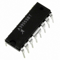
A3955SB-T Allegro Microsystems Inc, A3955SB-T Datasheet - Page 8

A3955SB-T
Manufacturer Part Number
A3955SB-T
Description
IC MOTOR DRIVER PWM FULL 16-DIP
Manufacturer
Allegro Microsystems Inc
Datasheet
1.A3955SB-T.pdf
(14 pages)
Specifications of A3955SB-T
Applications
Stepper Motor Driver
Number Of Outputs
1
Current - Output
±1.5A
Voltage - Load
4.5 V ~ 50 V
Voltage - Supply
4.5 V ~ 5.5 V
Operating Temperature
-20°C ~ 85°C
Mounting Type
Through Hole
Package / Case
16-DIP (0.300", 7.62mm)
Motor Type
Full Bridge
No. Of Outputs
2
Output Current
1.5A
Output Voltage
50V
Supply Voltage Range
4.5V To 5.5V
Driver Case Style
DIP
No. Of Pins
16
Lead Free Status / RoHS Status
Lead free / RoHS Compliant
Other names
620-1067
A3955
Two A3955 full-bridge PWM microstepping motor drivers are
needed to drive the windings of a bipolar stepper motor. Internal
pulse width modulated (PWM) control circuitry regulates each
motor winding current. The peak motor current is set by the
value of an external current-sense resistor (R
voltage (V
inputs (D
To improve motor performance, especially when using
sinusoidal current profi les necessary for microstepping, the
A3955 has three distinct current-decay modes: slow decay, fast
decay, and mixed decay.
PHASE Input.
current fl ow in the load (table 1). An internally generated dead
time of approximately 1 μs prevents crossover currents that
could occur when switching the PHASE input.
DAC Data Inputs (D
to digitally control the output current. The output of the DAC is
used to set the trip point of the current-sense comparator. Table 3
shows DAC output voltages for each input condition. When D
D
are turned off.
Internal PWM Current Control.
contains an internal fi xed off-time PWM current-control circuit
that limits the load current to a desired value (I
a diagonal pair of source and sink transistors are enabled and
current fl ows through the motor winding and R
the voltage across the sense resistor equals the DAC output
voltage the current-sense comparator resets the PWM latch,
1
, and D
0
2
, D
REF
are all logic low, all of the power output transistors
1
), and the digital-to-analog converter (DAC) data
Figure 1 — Load-Current Paths
, and D
Functional Description
R S
The PHASE input controls the direction of
2
).
V
BB
0
, D
1
, D
2
).
DRIVE CURRENT
RECIRCULATION
(SLOW-DECAY MODE)
RECIRCULATION
(FAST-DECAY MODE)
Full-Bridge PWM Microstepping Motor Driver
A non-linear DAC is used
Each motor driver
S
), a reference
Dwg. EP-006-15
TRIP
S
(fi gure 1). When
). Initially,
0
,
which turns off the source drivers (slow-decay mode) or the sink
and source drivers (fast- or mixed-decay mode).
With the DATA input lines tied to V
current limiting is set by the selection of R
transconductance function approximated by:
The actual peak load current (I
I
remain off for a time period determined by a user-selected
external resistor-capacitor combination (R
the fi xed off-time, the driver(s) are re-enabled, allowing the load
current to increase to I
current.
The DAC data input lines are used to provide up to eight levels
of output current. The internal 3-bit digital-to-analog converter
reduces the reference input to the current-sense comparator
in precise steps (the step reference current ratio or SRCR) to
provide half-step, quarter-step, or “microstepping” load-current
levels.
Slow Current-Decay Mode.
device is in slow current-decay mode (the source drivers are
disabled when the load current reaches I
off-time, the load inductance causes the current to recirculate
through the motor winding, sink driver, ground clamp diode,
and sense resistor (see fi gure 1). Slow-decay mode produces
low ripple current for a given fi xed off-time (see fi gure 2).
Low ripple current is desirable because the average current
in the motor winding is more nearly equal to the desired
TRIP
due to internal logic and switching delays. The driver(s)
Figure 2 — Current-Decay Waveforms
PFD
t
OFF
I
I
PEAK
TRIP
TRIP
I
TRIP
≈ SRCR x V
115 Northeast Cutoff
1.508.853.5000; www.allegromicro.com
Allegro MicroSystems, Inc.
Worcester, Massachusetts 01615-0036 U.S.A.
again, maintaining an average load
≈ V
PEAK
REF
) will be slightly higher than
When V
CC
/ 3R
REF
, the maximum value of
S
TRIP
/3R
.
SLOW (V
MIXED (1.1 V ≤ V
FAST (V
T
S
C
PFD
). During the fi xed
and V
S
T
). At the end of
PFD
≥ 3.5 V, the
PFD
≤ 0.8 V)
REF
≥ 3.5 V)
PFD
Dwg. WP-031-1
with a
≤ 3.1 V)
7


