LMD18245T/NOPB National Semiconductor, LMD18245T/NOPB Datasheet - Page 4
LMD18245T/NOPB
Manufacturer Part Number
LMD18245T/NOPB
Description
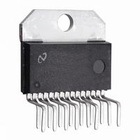
IC H BRIDGE 3A 55V TO-220
Manufacturer
National Semiconductor
Datasheet
1.LMD18245TNOPB.pdf
(21 pages)
Specifications of LMD18245T/NOPB
Applications
DC Motor Driver, Stepper Motor Driver, H Bridge
Number Of Outputs
1
Current - Output
3A
Voltage - Supply
12 V ~ 55 V
Operating Temperature
-40°C ~ 125°C
Mounting Type
Through Hole
Package / Case
TO-220-15 (Bent and Staggered Leads)
Operating Temperature Classification
Automotive
Package Type
TO-220
Operating Supply Voltage (min)
12V
Operating Supply Voltage (max)
55V
Lead Free Status / RoHS Status
Lead free / RoHS Compliant
Voltage - Load
-
Lead Free Status / Rohs Status
Compliant
Other names
*LMD18245T
*LMD18245T/NOPB
LMD18245T
*LMD18245T/NOPB
LMD18245T
Available stocks
Company
Part Number
Manufacturer
Quantity
Price
Company:

Part Number:
LMD18245T/NOPB
Manufacturer:
ST
Quantity:
14 300
Part Number:
LMD18245T/NOPB
Manufacturer:
NS/国半
Quantity:
20 000


www.national.com
CURRENT SENSE AMPLIFIER
DIGITAL-TO-ANALOG CONVERTER (DAC)
I
COMPARATOR AND MONOSTABLE
T
t
PROTECTION AND PACKAGE THERMAL RESISTANCES
LOGIC INPUTS
V
V
I
REF
DELAY
IN
JC
JA
Symbol
JSD
Electrical Characteristics
IL
IH
The following specifications apply for V
perature range, −40˚C
Note 1: Absolute Maximum Ratings indicate limits beyond which damage to the device may occur. Electrical specifications do not apply when operating the device
outside the rated Operating Conditions.
Note 2: Unless otherwise stated, load currents are pulses with widths less than 2 ms and duty cycles less than 5%.
Note 3: The maximum allowable power dissipation at any ambient temperature is P
operation, T
forcing T
junction-to-case thermal resistance of the package,
Note 4: ESD rating is based on the human body model of 100 pF discharged through a 1.5 k
800V.
Note 5: All limits are 100% production tested at 25˚C. Temperature extreme limits are guaranteed via correlation using accepted SQC (Statistical Quality Control)
methods. All limits are used to calculate AOQL (Average Outgoing Quality Level). Typicals are at T
Note 6: Asymmetric turn OFF and ON delay times and switching times ensure a switch turns OFF before the other switch in the same half H-bridge begins to turn
ON (preventing momentary short circuits between the power supply and ground). The transitional period during which both switches are OFF is commonly referred
to as the dead band.
Note 7: (I
The current sense linearity is specified as the slope of the line between the 0.5A and 1A data points minus the slope of the line between the 2A and 3A data points
all divided by the slope of the line between the 0.5A and 1A data points.
Note 8: Turn OFF delay, t
DMOS switch beginning to turn OFF. With V
5V at 1.2V/µs, and t
J
above 125˚C. If the junction temperature exceeds 155˚C, internal circuitry disables the power bridge. When a heatsink is used,
LOAD
A
is the ambient temperature in ˚C, and
Current Sense Offset
Resolution
Monotonicity
Total Unadjusted Error
Propagation Delay
DAC REF Input Current
Comparator High Output Level
Comparator Low Output Level
Comparator Output Current
Monostable Turn OFF Delay
Undervoltage Lockout, V
Shutdown Temperature, T
Package Thermal Resistances
Low Level Input Voltage
High Level Input Voltage
Input Current
, I
Source
Sink
Junction-to-Case, TO-220
Junction-to-Ambient, TO-220
SENSE
DELAY
) data points are taken for load currents of 0.5A, 1A, 2A and 3A. The current sense gain is specified as I
DELAY
is measured as the time from the voltage at RC reaching 2V to the time the voltage at OUT 1 reaches 3V.
Parameter
, is defined as the time from the voltage at the output of the current sense amplifier reaching the DAC output voltage to the lower
T
J
+125˚C. All other limits apply for T
CC
CC
= 32V, DIRECTION high, and 200
J
CC
JA
JC
= +42V, unless otherwise stated. Boldface limits apply over the operating tem-
(Note 2) (Continued)
is the junction-to-ambient thermal resistance in ˚C/W. Exceeding P
, and the case-to-ambient thermal resistance of the heatsink.
I
DAC REF = +5V
(Note 8)
V
LOAD
IN
= 0V or 12V
= 0A
Conditions
4
connected between OUT1 and V
A
Max
= T
= (125 − T
J
= 25˚C.
resistor. M1, M2, M3 and M4, pins 8, 7, 6 and 4 are protected to
J
A
= 25˚C and represent the most likely parametric norm.
)/
JA
, where 125˚C is the maximum junction temperature for
(Note 5)
Typical
0.125
−0.5
6.27
155
CC
0.2
3.2
1.2
1.5
50
88
35
5
, the voltage at RC is increased from 0V to
max
voids the Electrical Specifications by
SENSE
(Note 5)
Limit
/I
0.25
−0.1
±
±
LOAD
0.5
2.0
0.8
20
12
4
4
5
8
2
10
10
for the 1A data point.
JA
is the sum of the
LSB (max)
LSB (max)
Bits (min)
Bits (min)
µA (max)
µA (max)
µA (max)
µs (max)
(Limits)
V (max)
V (max)
V (max)
V (min)
V (min)
V (min)
Units
˚C/W
˚C/W
mV
mA
mA
µA
µA
ns
µs
˚C
V
Related parts for LMD18245T/NOPB
Image
Part Number
Description
Manufacturer
Datasheet
Request
R

Part Number:
Description:
IC MOTOR DRIVER FULL BRIDGE 3A TO-220-15
Manufacturer:
National Semiconductor
Datasheet:

Part Number:
Description:
H-BRIDGE MOTOR DRIVER W/ PWM
Manufacturer:
National Semiconductor
Part Number:
Description:
Manufacturer:
National Semiconductor
Datasheet:

Part Number:
Description:
3a, 55v Dmos Full-bridge Motor Driver
Manufacturer:
National Semiconductor Corporation
Datasheet:
Part Number:
Description:
National Semiconductor [8-Bit D/A Converter]
Manufacturer:
National Semiconductor
Datasheet:
Part Number:
Description:
National Semiconductor [Media Coprocessor]
Manufacturer:
National Semiconductor
Datasheet:
Part Number:
Description:
Digitally Controlled Tone and Volume Circuit with Stereo Audio Power Amplifier, Microphone Preamp Stage and National 3D Sound
Manufacturer:
National Semiconductor
Datasheet:
Part Number:
Description:
Digitally Controlled Tone and Volume Circuit with Stereo Audio Power Amplifier, Microphone Preamp Stage and National 3D Sound
Manufacturer:
National Semiconductor
Datasheet:
Part Number:
Description:
AC97 Rev 2 Codec with Sample Rate Conversion and National 3D Sound
Manufacturer:
National Semiconductor
Part Number:
Description:
Manufacturer:
National Semiconductor
Datasheet:
Part Number:
Description:
Manufacturer:
National Semiconductor
Datasheet:
Part Number:
Description:
General Purpose, Low Voltage, Low Power, Rail-to-Rail Output Operational Amplifiers
Manufacturer:
National Semiconductor
Datasheet:
Part Number:
Description:
8-bit 20 MSPS flash A/D converter.
Manufacturer:
National Semiconductor
Datasheet:
Part Number:
Description:
Low Noise Quad Operational Amplifier
Manufacturer:
National Semiconductor
Datasheet: