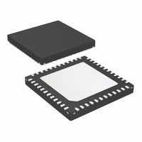
ATA6833-PLQW Atmel, ATA6833-PLQW Datasheet - Page 21

ATA6833-PLQW
Manufacturer Part Number
ATA6833-PLQW
Description
IC BLDC MOTOR DVR/LIN SBC 48VQFN
Manufacturer
Atmel
Type
3 Phase Brushless DC Motor Controllerr
Datasheet
1.ATA6833-PLQW.pdf
(27 pages)
Specifications of ATA6833-PLQW
Applications
DC Motor Controller, Brushless (BLDC), 3 Phase
Number Of Outputs
1
Voltage - Supply
5.5 V ~ 22.3 V
Operating Temperature
-40°C ~ 150°C
Mounting Type
Surface Mount
Package / Case
48-VQFN Exposed Pad, 48-HVQFN, 48-SQFN, 48-DHVQFN
Product
Fan / Motor Controllers / Drivers
Supply Current
7 mA
Mounting Style
SMD/SMT
Lead Free Status / RoHS Status
Lead free / RoHS Compliant
Current - Output
-
Voltage - Load
-
Lead Free Status / Rohs Status
Lead free / RoHS Compliant
8. Electrical Characteristics (Continued)
All parameters given are valid for 5.5V V
GND. (xxx) Values for the Atmel
9122G–AUTO–10/10
8.10
8.11
8.12
8.13
8.14
8.15
8.16
8.17
8.18
8.19 Fall time low-side driver
8.20 Rise time low-side driver
8.21
8.22
8.23 Fall time high-side driver
8.24 Rise time high-side driver
*) Type means: A = 100% tested, B = 100% correlation tested, C = Characterized on samples, D = Design parameter
No. Parameters
8.9
Output peak current at pins
Hx (switched from low to
high
Output peak current at pins
Hx (switched from high to
low)
Output peak current at pins
Lx (switched from low to
high
Output peak current at pins
Lx (switched from high to
low)
Output voltage low level
pins Hx
Output voltage high level
pins Hx
Sink resistance between Hx
and Sx
Sink resistance between Sx
and GND
Dynamic Parameters
Propagation delay time,
low-side driver from high to
low
Propagation delay time,
low-side driver from low to
high
Propagation delay time,
high-side driver from high
to low
Propagation delay time,
high-side driver from low to
high
®
ATA6834.
Test Conditions
V
V
C = 10nF
R = 1
V
V
C = 10nF
R = 1
V
V
C = 10nF
R = 1
V
V
C = 10nF
R = 1
V
I
I
V
C
V
C
V
C
V
C
Hx
Hx
Hx
VBAT
Hx
VBAT
Lx
VBAT
LX
VBAT
Sx
VBAT
VBAT
VBAT
VBAT
Gx
Gx
Gx
Gx
= 1mA
= –100µA
= 0V;
– V
= 10V;
= 0V
– V
= 5nF
= 5nF
= 5nF
= 5nF
= 7V – 20V
= 7 – 20V
= 7 – 20V
= 7 – 20V
= 13.5V
= 13.5V
= 13.5V,
= 13.5V,
VBAT
Sx
Sx
= 10V;
= 0V;
18V and for –40°C T
Atmel ATA6833/ATA6834 [Preliminary]
J
Sx to
GND
150°C (200°C) unless stated otherwise. All values refer to PIN
Pin
Symbol
V
R
R
t
t
I
V
HxHstat
t
t
I
I
I
HxHL
HxLH
HxH,
Hxsink
Sxsink
LxHL
LxLH
t
t
LxH,
t
t
HxL
LxL
Hxf
Hxr
Lxf
Lxr
HxL
V
VCPOUT
– 1V
Min.
200
200
45
Typ.
75
1
V
Max.
–200
–200
VCPOUT
115
0.3
0.9
0.9
0.3
0.3
0.9
0.9
0.3
0.3
Unit Type*
mA
mA
mA
mA
M
k
µs
µs
µs
µs
µs
µs
µs
µs
V
V
C
C
C
C
D
A
A
A
A
A
A
A
A
A
A
A
21


