ATA6834-PLQW Atmel, ATA6834-PLQW Datasheet - Page 8
ATA6834-PLQW
Manufacturer Part Number
ATA6834-PLQW
Description
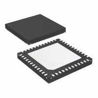
IC BLDC MOTOR DVR/LIN SBC 48VQFN
Manufacturer
Atmel
Type
3 Phase Brushless DC Motor Controllerr
Datasheet
1.ATA6833-PLQW.pdf
(27 pages)
Specifications of ATA6834-PLQW
Applications
DC Motor Controller, Brushless (BLDC), 3 Phase
Number Of Outputs
1
Voltage - Supply
5.5 V ~ 22.3 V
Operating Temperature
-40°C ~ 150°C
Mounting Type
Surface Mount
Package / Case
48-VQFN Exposed Pad, 48-HVQFN, 48-SQFN, 48-DHVQFN
Product
Fan / Motor Controllers / Drivers
Supply Current
7 mA
Mounting Style
SMD/SMT
Lead Free Status / RoHS Status
Lead free / RoHS Compliant
Current - Output
-
Voltage - Load
-
Lead Free Status / Rohs Status
Lead free / RoHS Compliant


3.4
Figure 3-4.
8
88% VCC
Reset and Watchdog Management
Atmel ATA6833/ATA6834 [Preliminary]
VCC
WD
/RESET
Timing Diagram of the Watchdog in Conjunction with the /RESET Signal
Reset and lead
time, no trigger
t
res
The watchdog timing is based on the trimmed internal watchdog oscillator. Its period time T
is determined by the external resistor R
function; a LOW signal disables it. Since WDD pin is equipped with an internal pull-up resistor
the watchdog is enabled by default. In order to keep the current consumption as low as possi-
ble the watchdog is switched off during Sleep Mode.
The timing diagram in
After power-up of the VCC regulator (VCC output exceeds 88% of its nominal value) /RESET
output stays LOW for the timeout period t
switches to HIGH. During the following time t
expected otherwise another external reset will be triggered.
When the watchdog has been correctly triggered for the first time, normal watch-dog operation
begins. A normal watchdog cycle consists of two time sections t
pulse for the time t
Rising edges on WD pin during t
is always the time of the last rising edge either on WD pin or on /RESET pin.
If the watchdog is disabled (WDD = LOW), only the initial reset for the time t
will be generated.
Additional resets will be generated if the VCC output voltage drops below 80% of its nominal
value.
The following example demonstrates how to calculate the timing scheme for valid watchdog
trigger pulses, which the external microcontroller has to provide in order to prevent undesired
resets.
t
d
trigger during lead time
Reset and lead time,
t
res
resshort
t
d
Figure 3-4
trigger edge
Watchdog
at /RESET if no valid trigger has been applied at pin WD during t
Watchdog cycle,
t
1
1
no trigger
shows the watchdog and external reset timing.
also cause a short pulse on /RESET. Start for such a cycle
WD
t
. A HIGH signal on WDD pin enables the watchdog
2
res
d
(typical 500ms) a rising edge at the input WD is
(typical 10ms). Subsequently /RESET output
t
Watchdog cycle, trigger
resshort
t
during t
1
2
1
window
and t
Watchdog trigger
t
2
in t
2
followed by a short
2
window
res
9122G–AUTO–10/10
after power-up
t
1
OSC
2
.
Related parts for ATA6834-PLQW
Image
Part Number
Description
Manufacturer
Datasheet
Request
R

Part Number:
Description:
BOARD BLDC MOTOR CTRL ATA6833/34
Manufacturer:
Atmel
Datasheet:

Part Number:
Description:
(ATA6833 / ATA6834) BLDC Motor Driver and LIN System Basis Chip
Manufacturer:
ATMEL Corporation
Datasheet:

Part Number:
Description:
DEV KIT FOR AVR/AVR32
Manufacturer:
Atmel
Datasheet:
Part Number:
Description:
INTERVAL AND WIPE/WASH WIPER CONTROL IC WITH DELAY
Manufacturer:
ATMEL Corporation
Datasheet:
Part Number:
Description:
Low-Voltage Voice-Switched IC for Hands-Free Operation
Manufacturer:
ATMEL Corporation
Datasheet:
Part Number:
Description:
MONOLITHIC INTEGRATED FEATUREPHONE CIRCUIT
Manufacturer:
ATMEL Corporation
Datasheet:
Part Number:
Description:
AM-FM Receiver IC U4255BM-M
Manufacturer:
ATMEL Corporation
Datasheet:
Part Number:
Description:
Monolithic Integrated Feature Phone Circuit
Manufacturer:
ATMEL Corporation
Datasheet:
Part Number:
Description:
Multistandard Video-IF and Quasi Parallel Sound Processing
Manufacturer:
ATMEL Corporation
Datasheet:
Part Number:
Description:
High-performance EE PLD
Manufacturer:
ATMEL Corporation
Datasheet:
Part Number:
Description:
8-bit Flash Microcontroller
Manufacturer:
ATMEL Corporation
Datasheet:
Part Number:
Description:
2-Wire Serial EEPROM
Manufacturer:
ATMEL Corporation
Datasheet: