TLE5206-2 Infineon Technologies, TLE5206-2 Datasheet
TLE5206-2
Specifications of TLE5206-2
TLE5206-2
TLE5206-2IN
TLE52062
TLE52062NK
Available stocks


Related parts for TLE5206-2


TLE5206-2 Summary of contents
Page 1
H-Bridge for DC-Motor Applications 1 Overview 1.1 Features • Delivers continuous 6 A peak current • Optimized for DC motor management applications • Operates at supply voltages typ. 200 mΩ ...
Page 2
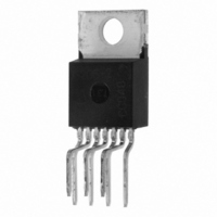
Pin Configuration (top view) TLE 5206 GND V OUT1 IN1 IN2 TLE 5206- OUT1 IN1 IN2 EF GND V S Figure 1 Data Sheet GND 1 N.C. ...
Page 3
Pin Definitions and Functions Pin No. Pin No. Symbol P-TO220 P-DSO 1 7 OUT1 IN1 4 1, 10, GND 11 IN2 OUT2 – ...
Page 4
Functional Block Diagram 2 EF Diagnosis and Protection Circuit 1 3 IN1 5 IN2 Diagnosis and Protection Circuit 2 Figure 2 Block Diagram Data Sheet Error Flag IN OUT ...
Page 5
Circuit Description Input Circuit The control inputs consist of TTL/CMOS-compatible schmitt-triggers with hysteresis. Buffer amplifiers are driven by this stages. Output Stages The output stages consist of a DMOS H-bridge. Integrated circuits protect the outputs against short-circuit to ground ...
Page 6
Monitoring Functions Undervoltage lockout (UVLO): V When reaches the switch on voltage S All output transistors are switched off if the supply voltage V value S OFF. 1.8 Protective Function Various errors like short-circuit to + result in turn-OFF ...
Page 7
Diagnosis Various errors as listed in the table “Diagnosis” are detected. Short circuits and overload result in turning off the output stages after a delay simultaneously [EF = L]. Changing the inputs to a state where the fault is ...
Page 8
Electrical Characteristics 3.1 Absolute Maximum Ratings – 40 °C < < 150 ° Parameter Voltages Supply voltage Logic input voltage Diagnostics output voltage Currents of DMOS-Transistors and Freewheeling Diodes Output current (cont.) Output current (peak) Output current ...
Page 9
Operating Range Parameter Supply voltage Supply voltage increasing Supply voltage decreasing Logic input voltage Junction temperature 3.3 Electrical Characteristics < < IN1 = IN2 = HIGH (No load); – 40 ...
Page 10
Electrical Characteristics (cont’ < < IN1 = IN2 = HIGH (No load); – 40 °C < I OUT1, 2 Parameter Outputs OUT1, 2 Static Drain-Source-On Resistance Source I = – ...
Page 11
Electrical Characteristics (cont’ < < IN1 = IN2 = HIGH (No load); – 40 °C < I OUT1, 2 Parameter Short Circuit Current Limitation Source current Sink current Output Delay ...
Page 12
Electrical Characteristics (cont’ < < IN1 = IN2 = HIGH (No load); – 40 °C < I OUT1, 2 Parameter Leakage Current Source Sink Logic Control Inputs ...
Page 13
IN1 V IN2 Figure 3 Test Circuit Overcurrent I I OUT SD Data Sheet Ι Ι 470 OUT1 IN1 3 TLE 5206-2 IN1 IN2 ...
Page 14
Ι OUT Source Ι OUT Sink Figure 4 Switching Time Definitions + 5 V Ω µ Figure 5 Application Circuit Data Sheet 50% t dONH 80% ...
Page 15
Application Modes 1. Simple CW/CCW-Control For low-cost application simple CW/CCW-Control without any speed regulation is recommended. A low-speed two-line interface is sufficient for the brake low, clockwise, counter clockwise and brake high command. 2. Sign/Magnitude Control For this mode two ...
Page 16
IN1, 2 Ι SCH Ι SDH Ι OUT1 Ι OUT1, 2 Short SCH t dSD EF Figure 7 Timing Diagram for Output Shorted to Ground IN1, 2 Ι SCL Ι SDL Ι OUT1 OUT1, ...
Page 17
Diagrams I Quiescent Current (active) S versus Junction Temperature 7 mA Ι - Input Switching Thresholds versus Junction Temperature 3 INH, L INH 2.5 2.0 V INL 1.5 1.0 ...
Page 18
Overcurrent Shutdown Threshold versus Junction Temperature 12 Ι Low Side Transistor 8 High Side Transistor - Data Sheet I Error-Flag Saturation Output Voltage versus Junction Temperature j EF AED02402 ...
Page 19
Package Outlines PG-TO220-7-11 (Plastic Transistor Single Outline Package) 0...0.3 0...0.15 1) Typical Metal surface min. X=7.25, Y=12.3 All metal surfaces tin plated, except area of cut. Green Product (RoHS compliant) To meet the world-wide customer requirements for environmentally friendly ...
Page 20
PG-DSO-20-37 (Plastic Dual Small Outline Package) 1.2 -0.3 1.27 +0.13 0 Index Marking 1 x 45˚ 15.9 1) Does not include plastic or metal protrusion of 0.15 max. per side Green Product (RoHS compliant) To meet the world-wide ...
Page 21
PG-TO263-7-1 (Plastic Transistor Single Outline Package) 0...0.3 7x0.6 ±0 Typical Metal surface min. X=7.25, Y=6.9 All metal surfaces tin plated, except area of cut. Green Product (RoHS compliant) To meet the world-wide customer requirements for environmentally friendly products ...
Page 22
PG-TO220-7-12 (Plastic Transistor Single Outline Package) 0...0.15 1) Typical Metal surface min. X=7.25, Y=12.3 All metal surfaces tin plated, except area of cut. Green Product (RoHS compliant) To meet the world-wide customer requirements for environmentally friendly products and to be ...
Page 23
Revision History Version Date Rev. 1.1 2007-07-31 RoHS-compliant version of the TLE 5206-2 Data Sheet Changes • All pages: Infineon logo updated • Page 1: “AEC qualified” and “RoHS” logo added, “Green Product (RoHS compliant)” and “AEC qualified” statement ...
Page 24
... Infineon Technologies Office. Infineon Technologies components may be used in life-support devices or systems only with the express written approval of Infineon Technologies failure of such components can reasonably be expected to cause the failure of that life-support device or system or to affect the safety or effectiveness of that device or system. Life support devices or systems are intended to be implanted in the human body or to support and/or maintain and sustain and/or protect human life ...