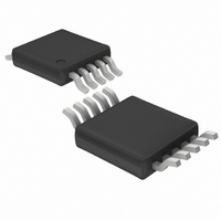
LT4351CMS#TRPBF Linear Technology, LT4351CMS#TRPBF Datasheet - Page 6

LT4351CMS#TRPBF
Manufacturer Part Number
LT4351CMS#TRPBF
Description
IC CTRLR MOSFET DIODE-OR 10MSOP
Manufacturer
Linear Technology
Datasheet
1.LT4351IMSPBF.pdf
(20 pages)
Specifications of LT4351CMS#TRPBF
Applications
Paralleled/Redundant Power Supplies
Fet Type
N-Channel
Number Of Outputs
1
Internal Switch(s)
No
Delay Time - Off
600ns
Voltage - Supply
1.2 V ~ 18 V
Current - Supply
1.4mA
Operating Temperature
0°C ~ 70°C
Mounting Type
Surface Mount
Package / Case
10-MSOP, Micro10™, 10-uMAX, 10-uSOP
Lead Free Status / RoHS Status
Lead free / RoHS Compliant
Delay Time - On
-
Available stocks
Company
Part Number
Manufacturer
Quantity
Price
LT4351
PIN FUNCTIONS
GATE (Pin 1): MOSFET Gate Drive Pin. This pin is tied to
the gate(s) of the external N-channel MOSFET(s). The GATE
pin drives high when UV is above the V
OV is below the V
OUT by 15mV. When not driven high, GATE actively pulls
to GND. GATE can sink or source up to 600mA.
V
pin for the gate drive amplifier. It is either generated by
the onboard boost regulator or supplied externally. When
turning on the MOSFET(s), a large high current pulse
flows through this pin. Bypass the pin with a 1µF capaci-
tor placed in close proximity to the part. The voltage on
this pin is also the feedback for the boost regulator. If the
V
switch is held off.
V
for the control circuitry and the boost regulator. It is also
one input in conjunction with OUT for controlling the
MOSFET(s). Bypassing should include a low ESR/ESL
capacitor placed in close proximity to the part.
SW (Pin 4): Boost Regulator Switch Pin. This pin is the
boost regulator switch output. It is connected to the boost
inductor and the boost diode. Peak switch current is limited
internally to 450mA. A Schottky diode between GND and
SW is required. If an external V
this pin open.
GND (Pin 5): Device Ground Pin. This pin is ground for the
boost switch, gate driver as well as the control circuitry.
Tie the V
close to this pin to minimize the effects of switching cur-
rents on part performance.
OV (Pin 6): Overvoltage Shutdown Pin. This pin is used
for input overvoltage detection. It is connected to a resis-
tive divider from V
threshold (0.3V), GATE is pulled to GND disabling power
transfer. In addition, the FAULT pin pulls low indicating a
6
DD
DD
IN
(Pin 3): Input Supply Pin. This pin is the supply pin
voltage exceeds the V
(Pin 2): Gate Drive Supply Pin. This is the supply
IN
and V
DD
OV(TH)
IN
bypass capacitors and ground plane
. When the voltage exceeds the OV
threshold and V
IN
voltage by 10.7V, the boost
DD
supply is used, leave
UV(TH)
IN
is greater than
threshold,
fault. Overvoltage detection has filtering on it to prevent
false triggering. The filtering depends on the level of over-
drive. Filtered tripping will occur when OV exceeds 0.3V.
If OV exceeds 0.33V, the gate immediately turns off (no
filtering). If overvoltage detection is not required, ground
the OV pin. See the Applications Information section for
further information.
UV (Pin 7): Undervoltage Shutdown Pin. This pin is used
for the undervoltage detect function. It is connected to
a resistive divider from V
the UV threshold, GATE pulls to GND disabling power
transfer. In addition, the FAULT pin pulls low indicating a
fault. When the UV pin voltage drops below the threshold,
a 10µA current is pulled from the divider to provide hys-
teresis. If undervoltage detection is not required, tie the
UV pin to a voltage greater than 320mV and not greater
than V
internal clamp. See the Applications Information section
for further information.
FAULT (Pin 8): Fault Comparator Status Pin. This pin pulls
low when a fault occurs. A fault has occurred if the UV pin
is below threshold or the OV pin is above threshold. The
FAULT pin low indicates that there is a problem with the
V
disabling the MOSFET(s) and prohibits common supply
contamination. If the GATE pin goes to compliance (GATE
equals the lesser of V
greater than OUT by more than 0.21V, FAULT turns on as
an indicator that the MOSFETs are probably not function-
ing. Leave this pin open if not used.
STATUS (Pin 9): MOSFET Status Pin. This pin pulls low
when GATE is above V
greater than OUT by 15mV. This indicates the MOSFET is
on. Leave this pin open if not used.
OUT (Pin 10): Common Supply Pin. This pin is connected
to the supply common and is used in conjunction with V
as one input controlling the MOSFET(s).
IN
(source) supply. GATE is pulled to GND during a fault,
IN
. Do not force more than 9V on UV due to an
DD
IN
– 2.3V or OUT + 7.4V) and V
IN
by more than 0.7V and V
. When the voltage is below
IN
IN
4351fc
is
is
IN


