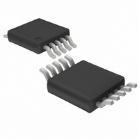
LT4351CMS#TRPBF Linear Technology, LT4351CMS#TRPBF Datasheet - Page 8

LT4351CMS#TRPBF
Manufacturer Part Number
LT4351CMS#TRPBF
Description
IC CTRLR MOSFET DIODE-OR 10MSOP
Manufacturer
Linear Technology
Datasheet
1.LT4351IMSPBF.pdf
(20 pages)
Specifications of LT4351CMS#TRPBF
Applications
Paralleled/Redundant Power Supplies
Fet Type
N-Channel
Number Of Outputs
1
Internal Switch(s)
No
Delay Time - Off
600ns
Voltage - Supply
1.2 V ~ 18 V
Current - Supply
1.4mA
Operating Temperature
0°C ~ 70°C
Mounting Type
Surface Mount
Package / Case
10-MSOP, Micro10™, 10-uMAX, 10-uSOP
Lead Free Status / RoHS Status
Lead free / RoHS Compliant
Delay Time - On
-
Available stocks
Company
Part Number
Manufacturer
Quantity
Price
OPERATION
LT4351
Increasingly, system designers have to deal with multiple
supply sources. The multiplicity may provide parallel,
redundant supplies for increased reliability or provide
a means of connecting disparate supplies. In all cases
the desire is for behavior like a diode but with no loss or
voltage drop.
ORing diodes have been the conventional means of con-
necting these supplies. The disadvantage of this approach
is that diodes introduce efficiency loss because of their
forward voltage drop. This variable voltage drop also de-
generates supply tolerance. Additionally, diodes provide
no information concerning the status of the sourcing
supply. Separate control must also be added to ensure
that a supply that is out of range is not allowed to affect
the common supply.
The LT4351 eliminates these problems by using N-channel
MOSFETs as the pass elements. The MOSFET is turned on
when power is being passed, allowing for a low voltage
drop from the supply to the load. When the input source
voltage drops below the output common supply voltage it
turns off the MOSFET, thereby matching the function and
performance of an ideal diode.
The LT4351 drives either a single MOSFET or dual back-
to-back MOSFETs. Dual MOSFETs are chosen to eliminate
current flow from the input supply to the output supply
when the V
A driver amplifier monitors the input (V
(OUT) and controls the MOSFETs. If V
by 15mV, GATE goes high and turns on the MOSFET(s)
allowing for power passage.
Undervoltage and overvoltage comparators C
and C
in conjunction with the UV and OV pins sets appropriate
thresholds such that the MOSFET(s) is off when the UV
pin is below 300mV or OV pin is above 300mV.
To help deal with the transients on the supply lines, the UV
input has current hysteresis. When the UV voltage drops
below the 300mV threshold, a 10µA current is pulled from
the pin. Thus the user can set the hysteresis level through
appropriate values in the divider.
Overvoltage shutdown occurs in two stages. The first oc-
curs when the OV pin exceeds the 300mV reference. When
8
OVF
also control power passage. A resistive divider
IN
voltage is greater than OUT.
IN
IN
exceeds OUT
) and output
UV
, C
OV
OV just exceeds the reference, an internal capacitor starts
charging, delaying the signal to turn off the MOSFET(s).
The second occurs when the OV pin exceeds 330mV. The
OVF comparator will immediately trip pulling GATE to GND.
This affords a delay inversely proportional to the amount of
overdrive. This also provides for glitch immunity without
compromising response time in the event of a serious
overvoltage condition.
The FAULT output indicates the status of the C
and C
tion. It also pulls low when GATE is at compliance and
V
nonfunctioning MOSFET. Compliance occurs when GATE
is at the lesser of OUT + 7.4V or V
its drive from the greater of V
or OUT is greater than 0.9V. If V
level, the output state is not guaranteed.
The gate drive consists of a high current, wide bandwidth
amplifier (driver). When the amplifier is enabled, it attempts
to regulate the GATE voltage such that the voltage across
the MOSFET(s) is approximately 15mV. If the MOSFET(s)
on resistance is so high as to prevent regulation, then
GATE goes to compliance and the MOSFET(s) fully turns
on. The inputs to the amplifier are V
pin sources current from V
The maximum GATE to V
2.3V or 7.4V above V
The STATUS comparator, ST, pulls low when GATE ex-
ceeds V
The STATUS pin pulls low as an indication that power is
passing through the MOSFET(s).
If V
or at compliance (GATE = V
high as an indication of a likely open MOSFET. FAULT will
pull low in this state indicating the probable fault.
The gate drive amplifier and STATUS function derive power
from V
the gate drive amplifier and STATUS are active independent
of the state of V
the event of V
(though of lesser strength) of GATE powered from OUT,
guaranteeing turn off.
IN
IN
> OUT by more than 0.21V indicating a probable
is greater than OUT by 0.21V and GATE > V
UV
DD
IN
. The circuit requires V
comparators. It pulls low during a fault condi-
by 0.7V. This occurs when V
DD
IN
collapse there still is an active pull-down
. If in a fault, GATE pulls actively low. In
OUT
IN
or V
DD
voltage is the lesser of V
DD
IN
IN
and sinks current to GND.
DD
– 2.3V), STATUS will go
(internal clamp voltage).
or OUT. It is active if V
DD
IN
> 2.5V. If V
IN
– 2.3V. FAULT derives
or OUT is below this
and OUT. The GATE
IN
> OUT + 15mV.
DD
is present,
OV
IN
+ 7.4V
, C
DD
4351fc
OVF
IN
–


