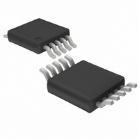
LTC4416EMS-1#PBF Linear Technology, LTC4416EMS-1#PBF Datasheet - Page 11

LTC4416EMS-1#PBF
Manufacturer Part Number
LTC4416EMS-1#PBF
Description
IC CNTRLR POWERPATH 10-MSOP
Manufacturer
Linear Technology
Series
PowerPath™r
Datasheet
1.LTC4416EMS-1PBF.pdf
(12 pages)
Specifications of LTC4416EMS-1#PBF
Applications
Battery Backup, Industrial/Automotive, High Current Switch
Fet Type
P-Channel
Number Of Outputs
2
Internal Switch(s)
No
Delay Time - On
60µs
Delay Time - Off
30µs
Voltage - Supply
3.6 V ~ 36 V
Current - Supply
130µA
Operating Temperature
-40°C ~ 85°C
Mounting Type
Surface Mount
Package / Case
10-MSOP, Micro10™, 10-uMAX, 10-uSOP
Lead Free Status / RoHS Status
Lead free / RoHS Compliant
Available stocks
Company
Part Number
Manufacturer
Quantity
Price
APPLICATIO S I FOR ATIO
Overvoltage
The over and undervoltage lockout circuits are shown here
working in tandem. It is possible to configure the circuit
for either over or undervoltage lockout by using only one
of the voltage paths and eliminating the components from
the other. Refer to Figure 7 for an LTC4416-1 configured
for overvotlage protection. If the input does not go below
ground, transistor Q1 can be eliminated.
The LTC4416-1 should be used in this configuration rather
than the LTC4416 because the LTC4416-1 will turn-off
rapidly if an over or undervoltage condition is detected.
Refer to Figure 8 for a comparison of the transient response
of the two ICs using the circuit configuration of Figure 6.
The LTC4416 will not turn-off quickly in an overvoltage
or undervoltage condition because the “fast-off” feature
is not enabled. This will cause the output to travel beyond
the desired range.
V
V
Figure 7. LTC4416-1 Configured for Overvoltage Protection
HYSTERESIS
FAIL
RESTORE
GND
V
V
TH2
IN
24.9k
=
=
WITH
R2C
1 222
V
.
ETH
=
=
1 222
V
•
.
R2A
221k
V
ETH
R A R c R E
R2E
187k
•
2
U
221 + +
•
R c R E
V
R A R c
+
2
R1A
100k
•
24 9
2
k
221
R c
||
2
H1
E1
GND
E2
H2
. ||
U
+
2
24 9
LTC4416-1
24 4 9
k
Information furnished by Linear Technology corporation is believed to be accurate and reliable.
However, no responsibility is assumed for its use. Linear Technology corporation makes no represen-
tation that the interconnection of its circuits as described herein will not infringe on existing patent rights.
k
2
||
+
. ||
2
.
187
24 9
2
k
k
G1
G2
V1
V
V2
.
S
187
k
W
k
=
k
Q1
12 07
=
13 51
.
Q2
.
4416 F07
V
U
V
V
TO
LOAD
OUT
Figure 9 contains a rapidly changing input voltage on a
much smaller time scale in comparison to Figure 8. The
LTC4416 will require the t
up current being applied. The gate voltage will be pulled
high with I
The discharge time of the gate will be dependent on the
capacitance of the external FET and the initial gate-source
voltage of the circuit. The total time delay will equal:
Figure 8. Transient Response of the LTC4416 vs the LTC4416-1
Light Load with a Large Capacitor on V
Figure 9. Close Up of the Transient Response of the LTC4416-1
to a Rapidly Rising Input
t
DELAY
20
15
10
13.60
13.55
13.50
13.45
13.40
G(OFF)
=
5
0
=
0
t
0
E OFF
t
E OFF
V
0
(
IN
(
LTC4416/LTC4416-1
which has a minimum current of 500µA.
5
)
)
+
20
+
t
10
DIScHARGE
c
LTC4416
I
GS
G
LTC4416-1
t
E(OFF)
TIME (ms)
E(OFF)
15
(
O O FF)
V
V
TIME (µs)
• ∆
OUT
40
IN
20
LTC4416
V
time prior to the rapid pull-
V
OUT
GATE DISCHARGE TIME
= C
25
OUT
60
I
G(OFF)
∆V
30
LTC4416-1
4416 F08
35
V
LTC4416-1
4416 F09
OUT
V
LTC4416
80
OUT
40
4416fa


