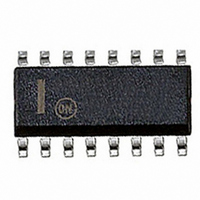
NCP1603D100R2 ON Semiconductor, NCP1603D100R2 Datasheet - Page 25

NCP1603D100R2
Manufacturer Part Number
NCP1603D100R2
Description
IC CTRLR PFC/PWM HV START 16SOIC
Manufacturer
ON Semiconductor
Datasheet
1.NCP1603D100R2.pdf
(30 pages)
Specifications of NCP1603D100R2
Mode
Critical Conduction (CRM), Discontinuous Conduction (DCM)
Frequency - Switching
58kHz
Current - Startup
17µA
Voltage - Supply
9 V ~ 18 V
Operating Temperature
-40°C ~ 125°C
Mounting Type
Surface Mount
Package / Case
16-SOIC (3.9mm Width)
Switching Frequency
405 KHz
Maximum Operating Temperature
+ 125 C
Mounting Style
SMD/SMT
Minimum Operating Temperature
- 40 C
Lead Free Status / RoHS Status
Contains lead / RoHS non-compliant
Other names
NCP1603D100R2OSTR
to make it reasonably close to zero, the setting of R
R
Figure 65 is studied here. When the inductor current is
exactly zero (i.e., I
Figure 65 is reached where R
Considering the tolerance, the actual sense resistor R
needed to be higher than the ideal value of R
ensure that zero current signal is generated when sense
current is smaller than the ZCD threshold (i.e., I
I
between the operating and ideal ZCD points in Figure 65.
Hence, R
recommended value of R
R
than R
Equation 23 with different inductor currents I
Equation 20 are studied.
Figure 66. When the inductor current I
I
hence the zero current signal is generated.
S(ZCD)
L(ZCD)
CS1
S(ZCD)
It is obvious that the I
Based on the CS pin (Pin 4) characteristics in Figure 35,
The higher value of R
Now that the R
These operating lines are added in Figure 65 to formulate
V
S(ZCD)
are crucial.
Figure 65. CS Pin Characteristic when I
). That is,
S(ZCD)
, the sense current I
that is 1.0 kW.
S1
has to be as low value as possible. The best
. From Equation 20, the operating lines in
V
R S u R S(ZCD) +
S
I
S(ZCD)
S1
V S + R S1 I S * R CS1 I L
L(ZCD)
is set at a particular value that is greater
L(ZCD)
R
Ideal ZCD point
S1
= 0), the ideal ZCD point in the
S1
R
S1
S1
S
is therefore the maximum of
S1
> R
Operating ZCD point
makes the bigger distance
is smaller than I
= R
is not always zero. In order
is R
S(ZCD)
S(ZCD)
V S(ZCD)
I S(ZCD)
S(ZCD)
L
(536 W typical).
is smaller than
L
S(ZCD)
= 0
S(ZCD)
(eq. 22)
(eq. 23)
http://onsemi.com
S1
L
S1
I
S
and
and
S
to
of
is
<
25
(R
lines to the line I
current sense resistor R
small as possible to minimize the error in the zero current
detection.
Overcurrent Protection (OCP) in PFC Section
I
is V
Drive Output of the device goes low.
Oscillator/Synchronization Block in PFC Section
Osc
S(OCP)
It is noted in Figure 66 and Equation 23 that when the
Overcurrent protection is reached when I
When overcurrent protection threshold is reached, the
CS1
V
S(OCP)
S(ZCD)
Figure 66. CS Pin Characteristic with Different
5
Figure 67. Oscillator / Synchronization Block
ZCD
point
Best
I
L
(200 mA typical). The offset voltage of the CS pin
45 mA
94 mA
) term is smaller the error or distance between the
I L(OCP) +
(3.2 mV typical) in this condition. That is:
0
V
I
S(ZCD)
S
1
L
5 V/3.5 V
= 0 is smaller. Therefore, the value of the
Oscillator Clock
Inductor Current
I
R S1 I S(OCP) * V S(OCP)
L
in PFC Section
+
−
= 0
CS1
I
L
is also recommended to be as
= I
R CS1
L(ZCD)
ZCD point
Operating
S
R
Zero Current
Q
delay
&
S
I
L
is larger than
> I
L(ZCD)
(eq. 24)
Turn on
MOSFET
I
S


