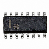
NCP1603D100R2 ON Semiconductor, NCP1603D100R2 Datasheet - Page 7

NCP1603D100R2
Manufacturer Part Number
NCP1603D100R2
Description
IC CTRLR PFC/PWM HV START 16SOIC
Manufacturer
ON Semiconductor
Datasheet
1.NCP1603D100R2.pdf
(30 pages)
Specifications of NCP1603D100R2
Mode
Critical Conduction (CRM), Discontinuous Conduction (DCM)
Frequency - Switching
58kHz
Current - Startup
17µA
Voltage - Supply
9 V ~ 18 V
Operating Temperature
-40°C ~ 125°C
Mounting Type
Surface Mount
Package / Case
16-SOIC (3.9mm Width)
Switching Frequency
405 KHz
Maximum Operating Temperature
+ 125 C
Mounting Style
SMD/SMT
Minimum Operating Temperature
- 40 C
Lead Free Status / RoHS Status
Contains lead / RoHS non-compliant
Other names
NCP1603D100R2OSTR
5. Comparator lower threshold is also the synchronization threshold.
ELECTRICAL CHARACTERISTICS
HV = 30 V, V
PWM SUPPLY SECTION
PFC OSCILLATOR
PFC GATE DRIVE
PFC FEEDBACK/OVERVOLTAGE PROTECTION/UNDERVOLTAGE PROTECTION
Supply Voltage
Startup Threshold, V
Minimum Operating Valley Voltage after Turn−On
Undervoltage Lockout Threshold Voltage, V
Logic Reset Level
Supply Current
Operating (V
Operating (V
Latch−Off Phase (V
Oscillator Frequency (Osc = 220 pF to GND)
Internal Capacitance of the Oscillator Pin
Maximum Oscillator Switching Frequency
Oscillator Discharge Current (Osc = 5.5 V)
Oscillator Charge Current (Osc = 3.0 V)
Comparator Lower Threshold (Osc = 220 pF to GND) (Note 5)
Comparator Upper Threshold (Osc = 220 pF to GND)
Synchronization Pulse Width for Detection
Synchronization Propagation Delay
Gate Drive Resistor
Output High and Draw 100 mA out of Out1 Pin
Output Low and Insert 100 mA into Out1 Pin
Gate Drive Rise Time from 1.5 V to 13.5 V
Gate Drive Fall Time from 13.5 V to 1.5 V
Reference Current
Regulation Block Ratio
Vcontrol Pin Internal Resistor
Maximum Control Voltage (I
Feedback Pin Voltage (I
Overvoltage Protection Current Ratio
Overvoltage Protection Current Threshold
Undervoltage Protection Current Threshold
(I
(I
(Out1 = 1.0 nF to GND)
(Out1 = 1.0 nF to GND)
source
sink
= 100 mA)
= 100 mA)
CC1
CC2
CC2
= 15 V, V
= 13 V, Out2 = Open, V
= 13 V, Out2 = 1.0 nF to GND2, V
Characteristic (PFC Section)
CC2
CC2
= 6.5 V, V
FB1
Increasing
control
FB1
= 100 mA)
= 100 mA)
= 100 nF, Ramp = 330 pF, Osc = 220 pF unless otherwise specified).
FB2
= 2.0 V)
FB2
(For typical values T
CC2
= 2.0 V)
Decreasing
FB2
= 2.0 V)
http://onsemi.com
J
= 25°C, for min/max values, T
7
Pin
14
14
10
10
5
5
5
5
5
5
5
5
5
7
7
7
9
9
9
9
9
9
V
V
V
I
f
V
t
control(max)
V
V
I
I
CC2(latch)
Symbol
osc1(max)
V
I
CC2(reset)
C
V
I
I
CC2(latch)
CC2(op1)
CC2(op2)
sync(min)
R
t
OVP
UVP
regL
FB1−100
CC2(on)
CC2(off)
sync(d)
R
sync(H)
R
f
osc(int)
I
sync(L)
I
control
I
osc1
odch
OVP
I
och
t
t
OH1
OL1
ref
r1
f1
/I
/I
/I
ref
ref
ref
J
= −40°C to +125°C, V
11.6
0.95
Min
400
500
192
104
7.0
5.0
0.6
1.3
3.0
4.5
5.0
2.0
4.0
52
40
40
95
−
−
−
−
−
−
−
−
−
12.6
11.6
1.05
Typ
680
405
371
203
300
107
217
7.7
5.6
4.0
1.1
2.2
3.5
5.0
7.2
3.0
8.0
58
36
49
45
53
32
96
−
CC2
= 13 V,
1000
Max
13.6
1.15
208
225
8.4
6.2
1.8
3.0
4.0
5.5
64
60
60
20
18
97
15
−
−
−
−
−
−
−
−
−
−
Unit
kHz
kHz
mA
mA
mA
mA
mA
mA
kW
mA
pF
ns
ns
ns
ns
W
W
%
%
%
V
V
V
V
V
V
V
V


