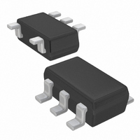
XC8101AA01MR Torex Semiconductor Ltd, XC8101AA01MR Datasheet - Page 7

XC8101AA01MR
Manufacturer Part Number
XC8101AA01MR
Description
IC HIGH SIDE LOAD SWITCH SOT25
Manufacturer
Torex Semiconductor Ltd
Type
High Side Switchr
Datasheet
1.XC8101AA01NR.pdf
(37 pages)
Specifications of XC8101AA01MR
Number Of Outputs
1
Rds (on)
1 Ohm
Internal Switch(s)
Yes
Current Limit
300mA
Voltage - Input
1.8 ~ 6 V
Operating Temperature
-40°C ~ 85°C
Mounting Type
Surface Mount
Package / Case
SOT-23-5, SC-74A, SOT-25
Lead Free Status / RoHS Status
Lead free / RoHS Compliant
<CE Pin>
The XC8101 enables an output P-channel MOSFET switch and the IC internal circuitry to turn off by the signal to the CE pin. In
The output voltage becomes unstable when the CE pin is opened. If the input voltage to the CE pin is within the specified
threshold voltages, the logic is fixed and the XC8101 will operate normally. However, supply current may increase as a result
of the shoot-through current of internal circuitry when the medium level voltage is input to the CE pin.
<Input Capacitor>
The XC8101 works well without an output capacitor (C
to the output side of the IC, input voltage ringing may occur when the IC is turned on. In order to reduce the ringing, an input
capacitor with the value of 1μF or more is requested to attach between V
placed as close as the IC.
<CL Auto-Discharge Function>
The XC8101A contains a C
XC8101A quickly discharge the electric charge in the output capacitor (C
whole IC circuit. . The C
capacitor (C
defined as (τ = C x R
<Current Limiter, Short-Circuit Protection>
The XC8101 series contains a constant current limiter and foldback current circuitry. The constant current limiter operates to
limit output current and the foldback current circuitry operates as short circuit protection for the output pin.
When the load current reaches the limit current, the constant current limiter operates and the output voltage drops. The output
voltage further, then the foldback current circuitry operates to decrease the output current. When the output pin is short-circuited
to the ground, the output current drops and maintains a flow about 30mA.
the shutdown mode, the V
■NOTES ON USE
1.
2.
3. V
■OPERATIONAL EXPLANATION
V: Output voltage after starting discharge
V
t: Discharge time
τ: Output discharge resistor value Rdischg×Output capacitor (C
OUT:
Please use this IC within the stated absolute maximum ratings. Operation beyond these limits may cause degrading or
permanent damage to the device.
The X8101 goes into an undefined operation when the CE pin is left open. The CE pin shall be tied to low or high level.
toward the V
OUT
Output voltage
pin voltage should not be applied beyond the V
L
) is determined by a CL auto-discharge resistor value (R
V = V
IN
OUT
pin.
DCHG
x e
L
auto-discharge resistance is set at 900Ω (V
–t/
). Output voltage after starting discharge can be calculated by the following formula.
OUT
L
τ
auto-discharge resistor and an N-channel transistor between the V
, or t=τIn (V
pin will be pulled down to the V
OUT
/ V)
L
). However, an output capacitor such as a bypass capacitor is tied up
IN
pin voltage. The IC may get damage due to the reverse current
SS
by the C
DCHG
L
OUT
) value C
L
) and an output capacitor value. Time constant τ is
L
) when a low signal to the CE pin is input to turn off a
=4.0V TYP. @ V
IN
auto-discharge function.
pin and V
SS
pin. The capacitor should be tied and
IN
=4.0). Discharge time of the output
OUT
pin and the V
SS
XC8101
pin. The
Series
7/37


