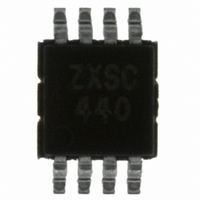
ZXSC440X8TA Diodes Zetex, ZXSC440X8TA Datasheet - Page 4

ZXSC440X8TA
Manufacturer Part Number
ZXSC440X8TA
Description
IC PHOTOFLASH CHARGER 8MSOP
Manufacturer
Diodes Zetex
Datasheet
1.ZXSC440X8TA.pdf
(16 pages)
Specifications of ZXSC440X8TA
Applications
Photoflash Capacitor Charger
Current - Supply
220µA
Voltage - Supply
1.8 V ~ 8 V
Operating Temperature
-40°C ~ 85°C
Mounting Type
Surface Mount
Package / Case
8-MSOP, Micro8™, 8-uMAX, 8-uSOP,
Lead Free Status / RoHS Status
Lead free / RoHS Compliant
Other names
ZXSC440X8TR
DEVICE DESCRIPTION
Bandgap reference
All threshold voltages and internal currents are derived
from a temperature compensated bandgap reference
circuit with a reference voltage of 1.22V nominal. If the
REF terminal is used as a reference for external
devices, the maximum load should not exceed ±2 A.
Dynamic drive output
Depending on the input signal, the output is either
"LOW" or "HIGH". In the high state a 3.4mA current
source (max drive voltage = V
or gate of the external transistor. In order to operate the
external switching transistor at optimum efficiency,
both output states are initiated with a short transient
current in order to quickly discharge the base or the
gate of the switching transistor.
Switching circuit
The switching circuit consists of two comparators,
Comp1 and Comp2, a gate U1, a monostable and the
drive output. Normally the DRIVE output is "HIGH"; the
external switching transistor is turned on. Current
ramps up in the inductor, the switching transistor and
external current sensing resistor. This voltage is
sensed by comparator, Comp2, at input SENSE. Once
the current sense voltage across the sensing resistor
exceeds 28mV, comparator, Comp2, through gate U1,
triggers a re-triggerable monostable and turns off the
output drive stage for 1.7 s. The inductor discharges
into the reservoir capacitor. After 1.7 s a new charge
cycle begins, thus ramping the output voltage. When
the output voltage reaches the nominal value and V
gets an input voltage of more than 300mV, the
monostable is forced "on" from Comp1 through gate
U1, until the feedback voltage falls below 300mV. The
above action continues to maintain regulation, with
slight hysteresis on the feedback threshold.
ZXSC440
S E M I C O N D U C T O R S
CC
-0.4V) drives the base
FB
4
READY detector
The READY circuit is a re-triggerable 195 s
monostable, which is re-triggered by every down
regulating action of comparator Comp1. As long as
regulation takes place, output READY is "HIGH" (high
impedance, 100K to V
voltage of less than 195 s are ignored. If the output
voltage falls below the nominal value for more than
195 s, output READY goes "LOW". This can be used to
signal to the camera controller that the flash unit has
charged fully and is ready to use.
CC
). Short dips of the output
ISSUE 1 - JANUARY 2005


