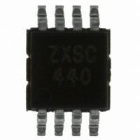
ZXSC440X8TA Diodes Zetex, ZXSC440X8TA Datasheet - Page 6

ZXSC440X8TA
Manufacturer Part Number
ZXSC440X8TA
Description
IC PHOTOFLASH CHARGER 8MSOP
Manufacturer
Diodes Zetex
Datasheet
1.ZXSC440X8TA.pdf
(16 pages)
Specifications of ZXSC440X8TA
Applications
Photoflash Capacitor Charger
Current - Supply
220µA
Voltage - Supply
1.8 V ~ 8 V
Operating Temperature
-40°C ~ 85°C
Mounting Type
Surface Mount
Package / Case
8-MSOP, Micro8™, 8-uMAX, 8-uSOP,
Lead Free Status / RoHS Status
Lead free / RoHS Compliant
Other names
ZXSC440X8TR
APPLICATIONS
Switching transistor selection
The choice of switching transistor has a major impact
on the converter efficiency. For optimum performance,
a bipolar transistor with low V
required. The V
important parameter as this sees typically three times
the input voltage when the transistor is switched off.
Zetex SuperSOT™ transistors are an ideal choice for
this application. At input voltages above 4V, suitable
Zetex MOSFET transistors will give almost the same
performance with a simpler drive circuit, omitting the
ZXTD6717 pre-drive stage.
Schottky diode may be omitted, as the body diode of
the MOSFET will perform the same function, with just a
small loss of efficiency.
Output rectifier diode selection
The diode should have a fast recovery, as any time
spent in reverse conduction removes energy from the
reservoir capacitor and dumps it, via the transformer,
into the protection diode across the output transistor.
This seriously reduces efficiency. Two BAS21 diodes
in series have been used, bearing in mind that the
reverse voltage across the diode is the sum of the
output voltage together with the input voltage
multiplied by the step-up ratio of the transformer:
Sense resistor
A low value sense resistor is required to set the peak
current. Power in this resistor is negligible due to the
low sense voltage threshold, V
recommended sense resistors:
Manufacturer
Cyntec
IRC
Using a 22m sense resistor results in a peak current of
just over 1.2A.
ZXSC440
S E M I C O N D U C T O R S
V
R(DIODE)
= V
CEO
of the switching transistor is also an
OUT(MAX)
Series
RL1220
LR1206
+ (V
SENSE
Using a MOSFET, the
CE(SAT)
IN
x T
. Below is a table of
and high gain is
URNS
R
0.022 - 10
0.010 - 1.0
DC
R
ATIO
( ) Range
)
6
Therefore, with a 300V output, a supply of 8 volts and a
1:12 step-up transformer, there will be a 396V across
the diode. This occurs during the current ramp-up in
the primary, as it transforms the input voltage up by the
turns ratio and the polarity at the secondary is such as
to add to the output voltage already being held off by
the diode.
Peak current definition
In general, the I
the switching transistor, Q1, is in full saturation with
maximum output power conditions, assuming
worse-case input voltage and transistor gain under all
operating temperature extremes.
Once I
determined by:
Size
0805
1206
R
SENSE
PK
is decided the value of R
=
V
Tolerance
±5%
±5%
SENSE
I
PK
PK
value must be chosen to ensure that
URL
http://www.cyntec.com
http://www.irctt.com
ISSUE 1 - JANUARY 2005
SENSE
can be


