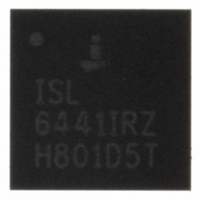
ISL6441IRZ-TK Intersil, ISL6441IRZ-TK Datasheet - Page 14

ISL6441IRZ-TK
Manufacturer Part Number
ISL6441IRZ-TK
Description
IC CTRLR PWM 1.4MHZ DUAL 28-QFN
Manufacturer
Intersil
Datasheet
1.ISL6441IRZ.pdf
(18 pages)
Specifications of ISL6441IRZ-TK
Applications
Power Supplies
Current - Supply
2mA
Voltage - Supply
5.6 V ~ 24 V
Operating Temperature
-40°C ~ 85°C
Mounting Type
Surface Mount
Package / Case
28-QFN
Rohs Compliant
YES
Lead Free Status / RoHS Status
Lead free / RoHS Compliant
Other names
ISL6441IRZ-TKTR
Available stocks
Company
Part Number
Manufacturer
Quantity
Price
Company:
Part Number:
ISL6441IRZ-TK
Manufacturer:
Intersil
Quantity:
2 400
Due to the current loop feedback, the modulator has a single
pole response with -20
by the load as shown in Equation 7.
where R
this type of modulator, a Type 2 compensation circuit is
usually sufficient.
Figure 19 shows a Type 2 amplifier and it’s response along
with the responses of the current mode modulator and the
converter. The Type 2 amplifier, in addition to the pole at
origin, has a zero-pole pair that causes a flat gain region at
frequencies in between the zero and the pole as shown in
Equations 8 and 9.
The zero frequency, the amplifier high-frequency gain, and
the modulator gain are chosen to satisfy most typical
applications. The crossover frequency will appear at the
point where the modulator attenuation equals the amplifier
high frequency gain. The only task that the system designer
has to complete is to specify the output filter capacitors to
position the load main pole somewhere within one decade
lower than the amplifier zero frequency. With this type of
compensation plenty of phase margin is easily achieved due
to zero-pole pair phase ‘boost’.
Conditional stability may occur only when the main load pole
is positioned too much to the left side on the frequency axis
due to excessive output filter capacitance. In this case, the
ESR zero placed within the 10kHz to 50kHz range gives
some additional phase ‘boost’. Some phase boost can also
be achieved by connecting capacitor C
F
F
F
Z
P
PO
MODULATOR
G
=
=
M
=
------------------------------ -
2π R
------------------------------ -
2π R
= 15.5dB
FIGURE 19. FEEDBACK LOOP COMPENSATION
-------------------------------- -
2π R
O
⋅
⋅
EA
1
⋅
is load resistance and C
1
F
2
1
CONVERTER
PO
1
⋅
⋅
O
C
C
⋅
1
2
C
=
=
O
10kHz
600kHz
dB
slope at a frequency determined
F
14
Z
R1
O
F
C
is load capacitance. For
G
EA
TYPE 2 EA
Z
R2
=13dB
in parallel with the
C2
C1
F
P
(EQ. 7)
(EQ. 8)
(EQ. 9)
ISL6441
upper resistor R
value. Please refer to the “Output Inductor Selection” and
the “Input Capacitor Selection on page 17 for further details.
Linear Regulator
The linear regulator controller is a trans conductance
amplifier with a nominal gain of 2A/V. The N-Channel
MOSFET output device can sink a minimum of 50mA. The
reference voltage is 0.8V. With 0V differential at its input, the
controller sinks 21mA of current. An external PNP transistor
or PFET pass element can be used. The dominant pole for
the loop can be placed at the base of the PNP (or gate of the
PFET), as a capacitor from emitter to base (source to gate of
a PFET). Better load transient response is achieved
however, if the dominant pole is placed at the output, with a
capacitor to ground at the output of the regulator.
Under no-load conditions, leakage currents from the pass
transistors supply the output capacitors, even when the
transistor is off. Generally this is not a problem since the
feedback resistor drains the excess charge. However,
charge may build up on the output capacitor making V
rise above its set point. Care must be taken to insure that the
feedback resistor’s current exceeds the pass transistor’s
leakage current over the entire temperature range.
The linear regulator output can be supplied by the output of
one of the PWMs. When using a PFET, the output of the
linear will track the PWM supply after the PWM output rises
to a voltage greater than the threshold of the PFET pass
device. The voltage differential between the PWM and the
linear output will be the load current times the r
Figure 20 shows the linear regulator (2.5V) start-up
waveform and the PWM (3.3V) start-up waveform.
FIGURE 20. LINEAR REGULATOR START-UP WAVEFORM
1
of the divider that sets the output voltage
V
V
OUT2
DS(ON)
OUT3
May 26, 2009
1V/DIV
1V/DIV
FN9197.3
LDO
.


