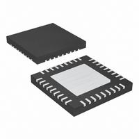
MAX8798ETX+ Maxim Integrated Products, MAX8798ETX+ Datasheet - Page 14

MAX8798ETX+
Manufacturer Part Number
MAX8798ETX+
Description
IC INTERNAL-SW BOOST REG 36-TQFN
Manufacturer
Maxim Integrated Products
Datasheet
1.MAX8798ETX.pdf
(31 pages)
Specifications of MAX8798ETX+
Applications
LCD Monitor, Notebook Display
Current - Supply
400µA
Voltage - Supply
1.8 V ~ 6 V
Operating Temperature
-40°C ~ 85°C
Mounting Type
Surface Mount
Package / Case
36-TQFN Exposed Pad
Operating Supply Voltage
1.8 V to 5.5 V
Maximum Operating Temperature
- 40 C
Mounting Style
SMD/SMT
Maximum Power Dissipation
2179.8 mW
Minimum Operating Temperature
+ 85 C
Supply Current
4 uA
Input Voltage
4V
Output Current
400mA
Output Voltage
18V
No. Of Outputs
2
Power Dissipation Pd
2.18W
Supply Voltage Range
1.8V To 5.5V
No. Of Pins
36
Operating Temperature Range
-40°C To +85°C
Rohs Compliant
Yes
Lead Free Status / RoHS Status
Lead free / RoHS Compliant
Internal-Switch Boost Regulator with
Integrated 3-Channel Scan Driver for TFT LCDs
14
28, 29
30, 31
PIN
20
21
22
23
24
25
26
27
32
33
34
35
36
—
______________________________________________________________________________________
BOOST
NAME
BGND
VCOM
COMP
AGND
PGND
GOFF
GON
OUT
NEG
POS
FB
LX
EP
IN
Amplifier Ground
Operational Amplifier Supply Input. Connect to V
greater ceramic capacitor.
Adjustable Sink-Current Output. OUT connects to the resistive voltage-divider at the op amp input POS
(between BOOST and GND) that determines the VCOM output voltage. I
a programmable amount.
Operational Amplifier Noninverting Input
Operational Amplifier Inverting Input
Operational Amplifier Output
Shutdown Control Input. Pull
and scan driver functions remain enabled.
Step-Up Regulator Supply Input. Bypass IN to AGND (pin 34) with a 1μF or greater ceramic capacitor.
Switching Node. Connect inductor/catch diode here and minimize trace area for lowest EMI.
Power Ground. Source connection of the internal step-up regulator power switch.
Feedback Input. Reference voltage is 1.24V nominal. Connect external resistor-divider
midpoint here and minimize trace area. Set V
Compensation Input for Error Amplifier. Connect a series RC from COMP to AGND. Typical values are
180k
Ground
Gate-Off Supply. GOFF is the negative supply voltage for the CKV, CKVB, and STVP high-voltage driver
outputs. Bypass to PGND with a minimum of 0.1μF ceramic capacitor.
Gate-On Supply. GON is the positive supply voltage for the CKV, CKVB, and STVP high-voltage driver
outputs. Bypass to V
Exposed Backside Pad. Connect to the analog ground plane through multiple vias to enhance thermal
performance.
and 470pF.
MAIN
or PGND with a minimum of 0.1μF ceramic capacitor.
low to disable the step-up regulator. The VCOM calibrator, op amp,
OUT
FUNCTION
MAIN
according to: V
(Figure 2) and bypass to BGND with a 1μF or
Pin Description (continued)
OUT
= 1.24V (1 + R1/R2).
OUT
lowers the divider voltage by


