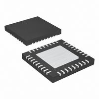
MAX8798ETX+ Maxim Integrated Products, MAX8798ETX+ Datasheet - Page 26

MAX8798ETX+
Manufacturer Part Number
MAX8798ETX+
Description
IC INTERNAL-SW BOOST REG 36-TQFN
Manufacturer
Maxim Integrated Products
Datasheet
1.MAX8798ETX.pdf
(31 pages)
Specifications of MAX8798ETX+
Applications
LCD Monitor, Notebook Display
Current - Supply
400µA
Voltage - Supply
1.8 V ~ 6 V
Operating Temperature
-40°C ~ 85°C
Mounting Type
Surface Mount
Package / Case
36-TQFN Exposed Pad
Operating Supply Voltage
1.8 V to 5.5 V
Maximum Operating Temperature
- 40 C
Mounting Style
SMD/SMT
Maximum Power Dissipation
2179.8 mW
Minimum Operating Temperature
+ 85 C
Supply Current
4 uA
Input Voltage
4V
Output Current
400mA
Output Voltage
18V
No. Of Outputs
2
Power Dissipation Pd
2.18W
Supply Voltage Range
1.8V To 5.5V
No. Of Pins
36
Operating Temperature Range
-40°C To +85°C
Rohs Compliant
Yes
Lead Free Status / RoHS Status
Lead free / RoHS Compliant
Table 5. DAC Settings
Internal-Switch Boost Regulator with
Integrated 3-Channel Scan Driver for TFT LCDs
The data byte follows successful transmission of the
MAX8798’s slave address (Figure 8). For a read opera-
tion, the MAX8798 outputs the 7 bits corresponding to
the current DAC setting followed by a 0 bit. For a write
operation, the bus master must provide the 7-bit data
corresponding to the desired DAC setting followed by a
1 bit. To program the IC’s EEPROM, the master must
make the last bit a zero. In this situation, the other 7 bits
of data are ignored. For programming, GON must
exceed its programming threshold. Otherwise, pro-
gramming does not occur and the MAX8798 does not
acknowledge the programming command.
Table 5 lists the DAC values and the corresponding
I
Figure 9. I
26
SET
0000000
0000001
.
.
.
1111110
1111111
DATA OUTPUT
DATA OUTPUT
DATA BYTE
BY MAX8798
BY MASTER
SCL FROM
, V
______________________________________________________________________________________
7-BIT
MASTER
SET
2
C Bus Acknowledge
, and V
CONDITION
I
I
1-LSB
.
.
.
I
1-LSB
I
SET(MAX)
SET(MAX)
SET(MIN)
SET(MIN)
OUT
START
S
I
SET
values.
+
-
V
V
1-LSB
.
.
.
V
1-LSB
V
SET(MAX)
SET(MAX)
SET(MIN)
SET(MIN)
V
SET
CLK1
D7
1
(V)
+
-
DAC Values
V
V
1-LSB
.
.
.
V
1-LSB
V
MIN
MIN
MAX
MAX
Data Byte
V
OUT
+
-
CLK2
D6
2
(V)
The MAX8798, when addressed, generates an acknowl-
edge pulse after the reception of each byte (Figure 9).
The master device must generate an extra clock pulse
that is associated with this acknowledge bit. The device
that acknowledges has to pull down the SDA line during
the acknowledge clock pulse so that the SDA line is sta-
ble LOW during the HIGH period of the acknowledge-
related clock pulse. Of course, setup and hold times
must be taken into account. The master signals an end
of data to the slave by not generating an acknowledge
bit on the last byte that has been clocked out of the
slave. In this case, the slave leaves the data line HIGH to
enable the master to generate the STOP condition.
The MAX8798 does not generate an acknowledge
while an internal programming cycle is in progress.
Once the internally timed write cycle has started and
the EEPROM inputs are disabled, acknowledge polling
can be initiated. This involves sending a START condi-
tion followed by the device address byte. Only if the
internal write cycle has completed does the MAX8798
respond with an acknowledge pulse, allowing the read
or write sequence to continue.
The MAX8798 does not acknowledge a command to
program the EEPROM if V
properly program the device. Also, a program com-
mand must be preceded by a write command. The IC
does not acknowledge a program command or pro-
gram the EEPROM unless the DAC data has been
modified since the most recent program command.
ACKNOWLEDGE
NOT ACKNOWLEDGE
CLK8
D0
8
GON
ACKNOWLEDGE
CLOCK PULSE
Acknowledge/Polling
is not high enough to
CLK9
9


