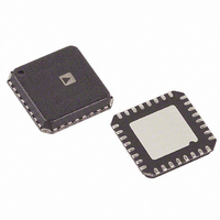
ADN8831ACPZ-R2 Analog Devices Inc, ADN8831ACPZ-R2 Datasheet - Page 10

ADN8831ACPZ-R2
Manufacturer Part Number
ADN8831ACPZ-R2
Description
IC THERMO COOLER CTRLR 32-LFCSP
Manufacturer
Analog Devices Inc
Datasheet
1.ADN8831ACPZ-REEL7.pdf
(20 pages)
Specifications of ADN8831ACPZ-R2
Applications
Thermoelectric Cooler
Current - Supply
8mA
Voltage - Supply
3 V ~ 5.5 V
Operating Temperature
-40°C ~ 85°C
Mounting Type
Surface Mount
Package / Case
32-LFCSP
Laser Driver Type
Thermoelectric Cooler
Supply Current
8mA
Supply Voltage Range
3V To 5.5V
Driver Case Style
LFCSP
No. Of Pins
32
Msl
MSL 1 - Unlimited
Supply Current Max
15mA
Device Type
Laser Diode
Rohs Compliant
Yes
Lead Free Status / RoHS Status
Lead free / RoHS Compliant
ADN8831
THEORY OF OPERATION
The ADN8831 is a controller for a thermoelectric cooler (TEC).
The voltage applied to the input of the ADN8831 corresponds
to the target temperature set point. The appropriate current is
then applied to the TEC to pump heat either to, or away from,
the object whose temperature is being regulated. The temperature
of the object is measured by a thermistor and is fed back to the
ADN8831 to correct the loop and settle the TEC to the appropriate
final temperature. For best stability, the thermistor should be
mounted in close proximity to the object. In most laser diode
modules, the TEC and thermistor are already mounted in the
unit and are used to regulate the temperature of the laser diode.
The ADN8831 integrates self-correcting auto-zero amplifiers
(Chop1 and Chop2). The Chop1 amplifier can be used as a
temperature measurement amplifier to create a voltage that is
proportional to the object temperature. The output of the tem-
perature measurement amplifier (Chop1) is then fed into the
compensation amplifier (Chop2). In a compensation stage, the
temperature measurement voltage is compared against the
temperature set input voltage, creating an error voltage that
is proportional to the difference. Also, an external network
THERMISTOR
TEMPERATURE SET INPUT
TEMP GOOD INDICATOR
TEC CURRENT OUTPUT
TEC VOLTAGE OUTPUT
17.8kΩ
7.68kΩ
27nF
17.8kΩ
10kΩ
0.1μF
8.2kΩ
8.2kΩ
10kΩ
10kΩ
10kΩ
30.1kΩ
10kΩ
10kΩ
10μF
TMPGD
VREF
VLIM
ILIMC
ILIMH
IN1P
IN1M
OUT1
IN2M
OUT2
IN2P
VTEC
ITEC
Figure 12. Typical Application Circuit 1
AVDD
Rev. 0 | Page 10 of 20
AGND
0.1μF
PGND
PVDD
consisting of several resistors and capacitors is connected
around the compensation amplifier. The user can adjust this
network to optimize the step response of the TEC temperature,
either in terms of settling time or maximum current change.
Details of how to adjust the compensation network are in the
PID Compensation Amplifier (Chop2) section. The TEC is
differentially driven using an H-bridge configuration. The
ADN8831 drives external transistors that are used to provide
the current to the TEC. To further improve the power efficiency
of the system, one side of the H-bridge uses a switched output.
Only one inductor and one capacitor are required to filter out
the switching frequency. The other side of the H-bridge uses
linear output without requiring any additional circuitry. This
proprietary configuration allows the ADN8831 to provide
efficiency of >90%. For most applications, a 4.7 μH inductor, a
22 μF capacitor, and a switching frequency of 1 MHz maintain
less than 0.5% worst-case output voltage ripple across the TEC.
The maximum voltage across the TEC and current flowing
through the TEC can be set using the VLIM and ILIM pins.
Additional details are in the Maximum TEC Voltage Limit and
Maximum TEC Current Limit sections.
COMPOSC
SYNCI/SD
COMPSW
SNGATE
LNGATE
SPGATE
LPGATE
SYNCO
PHASE
0.1μF
SS/SB
FREQ
SFB
LFB
SW
CS
118kΩ
10kΩ
0.1μF
10nF
1kΩ
NC
NC
0.1μF
VDD
3.0V TO 5.5V
22μH
3.3μH
VDD
22μF
TEC
R
SENSE


