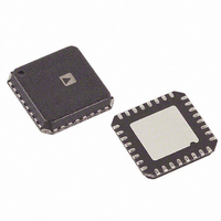
ADN8831ACPZ-R2 Analog Devices Inc, ADN8831ACPZ-R2 Datasheet - Page 11

ADN8831ACPZ-R2
Manufacturer Part Number
ADN8831ACPZ-R2
Description
IC THERMO COOLER CTRLR 32-LFCSP
Manufacturer
Analog Devices Inc
Datasheet
1.ADN8831ACPZ-REEL7.pdf
(20 pages)
Specifications of ADN8831ACPZ-R2
Applications
Thermoelectric Cooler
Current - Supply
8mA
Voltage - Supply
3 V ~ 5.5 V
Operating Temperature
-40°C ~ 85°C
Mounting Type
Surface Mount
Package / Case
32-LFCSP
Laser Driver Type
Thermoelectric Cooler
Supply Current
8mA
Supply Voltage Range
3V To 5.5V
Driver Case Style
LFCSP
No. Of Pins
32
Msl
MSL 1 - Unlimited
Supply Current Max
15mA
Device Type
Laser Diode
Rohs Compliant
Yes
Lead Free Status / RoHS Status
Lead free / RoHS Compliant
OSCILLATOR CLOCK FREQUENCY
The ADN8831 has an internal oscillator to generate the switching
frequency for the output stage. This oscillator can be set in either
free-run mode or synchronized to an external clock signal.
Free-Run Operation
The switching frequency is set by a single resistor connected
from FREQ (Pin 13) to ground.
common switching frequencies. For free-run operation, connect
SYNCI/ SD (Pin 16) and COMPOSC (Pin 17) to PVDD.
Table 5. Switching Frequencies vs. R
f
250 kHz
500 kHz
750 kHz
1 MHz
Higher switching frequencies reduce the voltage ripple across
the TEC. However, high switching frequencies will create more
power dissipation in the external transistors due to the more
frequent charging and discharging of the transistor gate
capacitances.
External Clock Operation
The switching frequency of the ADN8831 can be synchronized
with an external clock. Connect the clock signal to SYNCI/ SD
(Pin 16) and connect the COMPOSC (Pin 17) to an R-C
network. This network compensates a PLL to lock on to the
external clock.
SWITCH
ADN8831
Figure 14. Synchronize to an External Clock
ADN8831
Figure 13. Free-Run Mode
COMPOSC
SYNCI/SD
FREQ
COMPOSC
SYNCI/SD
FREQ
Table 5 shows R
R
484 kΩ
249 kΩ
168 kΩ
118 kΩ
1MΩ
1kΩ
FREQ
FREQ
1nF
R
FREQ
EXT. CLOCK
0.1μF
V
V
SOURCE
DD
DD
FREQ
for some
Rev. 0 | Page 11 of 20
Connecting Multiple ADN8831 Devices
Connecting the SYNCO to the SYNCI/ SD pin of another
ADN8831 allows multiple ADN8831 devices to be driven using
a single clock. Multiple ADN8831 devices can be driven from
either a single master ADN8831 device by connecting its
SYNCO pin to each slave SYNCI/
connecting each device’s SYNCO to the next device’s SYNCI/
pin. When multiple ADN8831 devices are clocked at the same
frequency, adjust its phase to reduce power supply ripple.
OSCILLATOR CLOCK PHASE
Adjust the oscillator clock phase using a simple resistor divider
at the PHASE pin. Phase adjustment allows two or more
ADN8831 devices to operate from the same clock frequency
and not have all outputs simultaneously switch, potentially
creating an excessive power supply ripple.
To ensure the correct operation of the oscillator, V
remain between 100 mV and 2.4 V. The PHASE pin is internally
biased at 1.2 V. If the PHASE pin is left open, clock phase is set
at 180° as the default.
Figure 15. Multiple ADN8831 Devices Driven from a Master Clock
ADN8831
MASTER
SYNCO
10kΩ
ADN8831
SLAVE
ADN8831
SLAVE
SYNCI/SD
SYNCI/SD
COMPOSC
SYNCI/SD
PHASE
FREQ
COMPOSC
COMPOSC
V
DD
PHASE
PHASE
FREQ
FREQ
SD pin, or daisy-chained by
118kΩ
V
V
NC
DD
DD
1MΩ
1MΩ
1kΩ
1kΩ
V
V
1nF
1nF
PHASE
PHASE
0.1μF
0.1μF
ADN8831
PHASE
should
SD


