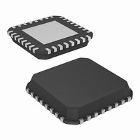
ISL97642IRTZ-T Intersil, ISL97642IRTZ-T Datasheet

ISL97642IRTZ-T
Specifications of ISL97642IRTZ-T
Available stocks
Related parts for ISL97642IRTZ-T
ISL97642IRTZ-T Summary of contents
Page 1
... LCD-TVs Ordering Information PART NUMBER (Note) ISL97642IRTZ* *Add “-T” or “-TK” suffix for tape and reel. Please refer to TB347 for details on reel specifications. NOTE: Intersil Pb-free plus anneal products employ special Pb-free material sets; molding compounds/die attach materials and 100% matte tin plate termination finish, which are RoHS compliant and compatible with both SnPb and Pb-free soldering operations ...
Page 2
Pinouts 2 ISL97642 ISL97642 (32 LD TQFN) TOP VIEW SRC 1 REF 2 AGND 3 PGND 4 THERMAL PAD OUT1 5 NEG1 6 POS1 7 OUT2 NOT INTERNALLY CONNECTED 24 COMP ...
Page 3
... Soft-Start Period SS 3 ISL97642 Thermal Information = +25°C) Storage Temperature . . . . . . . . . . . . . . . . . . . . . . . .-65°C to +150°C +0.3V Maximum Continuous Junction Temperature . . . . . . . . . . . . +125°C IN Power Dissipation . . . . . . . . . . . . . . . . . . . . . . . . . . . . . See Curves Operating Ambient Temperature . . . . . . . . . . . . . . . .-40°C to +85°C Pb-free reflow profile . . . . . . . . . . . . . . . . . . . . . . . . . .see link below http://www.intersil.com/pbfree/Pb-FreeReflow.asp -20V to V +0. +0.3V SRC = 12V 20V, Over-temperature from -40° ...
Page 4
Electrical Specifications Unless Otherwise Specified. (Continued) PARAMETER DESCRIPTION OPERATIONAL AMPLIFIERS V Supply Operating Range SUP I Supply Current per Amplifier SUP V Offset Voltage OS I Input Bias Current B CMIR Common Mode Input Range ...
Page 5
Electrical Specifications Unless Otherwise Specified. (Continued) PARAMETER DESCRIPTION I CTL CTL Input Leakage Current LEAK t rise CTL to OUT Rising Prop Delay D t fall CTL to OUT Falling Prop Delay D V SRC ...
Page 6
Pin Descriptions PIN NAME ISL97642 SRC 1 REF 2 AGND 3 PGND 4 OUT1 5 NEG1 6 POS1 7 OUT2 8 NEG2 9 POS2 10 BGND 11 POS3 15 NEG3 16 OUT3 17 SUP 14 POS3 15 NEG3 16 OUT3 ...
Page 7
Typical Performance Curves 100 200 400 600 800 LOAD CURRENT (mA) FIGURE 1. BOOST EFFICIENCY ...
Page 8
Typical Performance Curves 0 -0.05 -0.10 -0.15 -0.20 -0. LOAD CURRENT (mA) ON FIGURE 7. V LOAD REGULATION ON 0 -0.1 -0.2 -0.3 -0.4 -0.5 -0.6 -0.7 -0.8 -0 LOAD CURRENT ...
Page 9
Typical Performance Curves JEDEC JESD51-7 HIGH EFFECTIVE THERMAL CONDUCTIVITY TEST BOARD - QFN EXPOSED DIEPAD SOLDERED TO PCB PER JESD51-5 3.0 2.857W 2.5 QFN32 2.0 θ = 35°C/W JA 1.5 1.0 0 100 AMBIENT ...
Page 10
V REF REFERENCE GENERATOR FBB GM AMPLIFIER C INT UVLO COMPARATOR THERMAL SHUTDOWN DRVN BUFFER FBN 0.4V Boost Converter The main boost converter is a current mode PWM converter operating at a fixed frequency. The 1.2MHz switching frequency enables the ...
Page 11
The current through MOSFET is limited to 2.8A (typ) peak. This restricts the maximum output current based on Equation 3: ΔI V ⎛ ⎞ × -------- --------- – ⎝ ⎠ OMAX LMT ...
Page 12
Table 2 gives typical values (margins are considered 10%, 3%, 20%, 10% and 15 TABLE 2. V (V) V (V) L (µ 3.3 9 6.8 3.3 12 ...
Page 13
LDO_ON 0.9V PG_LDOP + 36V ESD - CLAMP R BP 700Ω DRVP FBP + - GMP 1: Np FIGURE 18. V FUNCTIONAL BLOCK DIAGRAM ON LDO_OFF PG_LDON - + R 0.4V 20kΩ FBN DRVN + GMN ...
Page 14
ISL97642 FIGURE 21. THE LINEAR REGULATOR CONTROLS ONE STAGE OF CHARGE PUMP Calculation of the Linear Regulator Base-emitter Resistors (RBP and RBN) For the pass transistor of the linear regulator, low frequency gain (Hfe) and unity gain frequency (f T ...
Page 15
V and V regulation – depending ON OFF on their exact loading conditions at the time. To optimize V /V ...
Page 16
V CDEL IN V REF V BOOST V OFF CIRCUIT ON SLICE NOTE: Not to scale Component Selection for Start-up Sequencing and Fault Protection The C capacitor is typically set at 220nF and is required REF to ...
Page 17
The user is directed to the layout guidelines and component selection sections to avoid problems during initial evaluation and prototype PCB generation. V -Slice Circuit ON The V -slice Circuit functions as a three ...
Page 18
Typical Application Circuit V IN (2.6V TO 5.5V) 10µF 10Ω C1 470nF 180Ω 2.2nF 700Ω 0.1µF Q21 V 82kΩ R22 NEG (-8V) 10kΩ 470nF R21 0.1µF CONTROL INPUT 100nF V MAIN V COM FB3 V COM3 V COM ...
Page 19
... Accordingly, the reader is cautioned to verify that data sheets are current before placing orders. Information furnished by Intersil is believed to be accurate and reliable. However, no responsibility is assumed by Intersil or its subsidiaries for its use; nor for any infringements of patents or other rights of third parties which may result from its use ...


