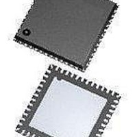
MAX16065ETM+ Maxim Integrated Products, MAX16065ETM+ Datasheet - Page 42

MAX16065ETM+
Manufacturer Part Number
MAX16065ETM+
Description
IC SYSTEM MANAGER 12CH 48-TQFN
Manufacturer
Maxim Integrated Products
Datasheet
1.MAX16065ETM.pdf
(62 pages)
Specifications of MAX16065ETM+
Applications
Power Supply Monitor, Sequencer
Voltage - Supply
2.8 V ~ 14 V
Current - Supply
4.5mA
Operating Temperature
-40°C ~ 85°C
Mounting Type
Surface Mount
Package / Case
48-TQFN Exposed Pad
Number Of Voltages Monitored
12
Undervoltage Threshold
2.7 V
Manual Reset
Resettable
Watchdog
Yes
Battery Backup Switching
No
Power-up Reset Delay (typ)
200 us
Supply Voltage (max)
14 V
Supply Voltage (min)
2.8 V
Supply Current (typ)
10 mA
Maximum Power Dissipation
2222 mW
Mounting Style
SMD/SMT
Maximum Operating Temperature
+ 85 C
Chip Enable Signals
No
Internal Hysteresis
Yes
Minimum Operating Temperature
- 40 C
Power Fail Detection
No
Lead Free Status / RoHS Status
Lead free / RoHS Compliant
Voltage - Input
-
Lead Free Status / Rohs Status
Lead free / RoHS Compliant
12-Channel/8-Channel, Flash-Configurable System
Managers with Nonvolatile Fault Registers
Flash must be written to 8 bytes at a time. The initial
address must be aligned to 8-byte boundaries—the 3
LSBs of the initial address must be ‘000’. Write the 8
bytes using a single block-write command or using 8
successive Write Byte commands.
The send byte protocol allows the master device to
send one byte of data to the slave device (see Figure
14). The send byte presets a register pointer address
for a subsequent read or write. The slave sends a NACK
instead of an ACK if the master tries to send a memory
address or command code that is not allowed. If the
master sends A5h or A6h, the data is ACK, because this
could be the start of the write block or read block. If the
master sends a STOP condition before the slave asserts
an ACK, the internal address pointer does not change.
If the master sends A7h, this signifies a software reboot.
The send byte procedure is the following:
1) The master sends a START condition.
2) The master sends the 7-bit slave address and a write
3) The addressed slave asserts an ACK on SDA.
4) The master sends an 8-bit memory address or com-
Figure
42
bit (low).
mand code.
TRANSMITTER
_____________________________________________________________________________________
13. Acknowledge
RECEIVER
SDA BY
SDA BY
SCL
S
Restrictions When Writing to Flash
1
Send Byte
2
5) The addressed slave asserts an ACK (or NACK)
6) The master sends a STOP condition.
The receive byte protocol allows the master device to
read the register content of the MAX16065/MAX16066
(see Figure 14). The flash or register address must be
preset with a send byte or write word protocol first. Once
the read is complete, the internal pointer increases by
one. Repeating the receive byte protocol reads the con-
tents of the next address. The receive byte procedure
follows:
1) The master sends a START condition.
2) The master sends the 7-bit slave address and a read
3) The addressed slave asserts an ACK on SDA.
4) The slave sends 8 data bits.
5 The master asserts a NACK on SDA.
6) The master generates a STOP condition.
The write byte protocol (see Figure 14) allows the mas-
ter device to write a single byte in the default page,
extended page, or flash page, depending on which
on SDA.
bit (high).
CLOCK PULSE FOR ACKNOWLEDGE
8
NACK
ACK
9
Receive Byte
Write Byte


