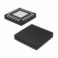
ISL6123IRZA-T Intersil, ISL6123IRZA-T Datasheet - Page 20

ISL6123IRZA-T
Manufacturer Part Number
ISL6123IRZA-T
Description
IC POWER SUPPLY SEQUENCER 24QFN
Manufacturer
Intersil
Datasheet
1.ISL6123IRZA.pdf
(22 pages)
Specifications of ISL6123IRZA-T
Applications
Power Supply Sequencer
Voltage - Supply
1.5 V ~ 5.5 V
Current - Supply
200µA
Operating Temperature
-40°C ~ 85°C
Mounting Type
Surface Mount
Package / Case
24-VQFN
Lead Free Status / RoHS Status
Lead free / RoHS Compliant
Voltage - Input
-
Available stocks
Company
Part Number
Manufacturer
Quantity
Price
Negative Voltage Sequencing
The ISL612X family can use the charged pump GATE output
to drive FETs that would control and sequence negative
voltages down to a nominal -5V with minimal additional
external circuitry. Figure 23 shows turn-on of 5V bipolar
supplies together, then the +2.5V and turn-off of both
positive supplies being turned off together after the -5V.
Figure 24 shows the minimal additional external circuitry to
accomplish this. The 5V zener diode is used to level shift the
GATE drive down 5V to prevent premature turn-on when
GATE = 0V. Once GATE drive voltage > Vz, then FET
Vgs > 5V, ensuring full turn-on once GATE gets to
VDD+5.3V. Turn-on and turn-off ramp rate can be adjusted
with FET gate series resistor value. Sequencing of the -V rail
is accomplished as normal via the DLY_X capacitor value
although adjustments in prototyping should be factored in to
fine tune for actual circuit requirements.
Figures 25 and 26 illustrate a high accuracy -V detection
circuit using the ISL6131 and a low cost low accuracy -V
detect circuit respectively.
ISL612X GATE
D1 necessary to prevent premature turn-on. R1 is used to hold
FET Vgs = 0V until D1 Vz is overcome. R1 value can be changed to
adjust -V ramp rates. Choose a R1 value between 4MΩ and 10MΩ
initially and fine tune resistor value for the particular need.
-V
FIGURE 24. -VOLTAGE FET DRIVE CIRCUIT
IN
FIGURE 23. ±VOLTAGE SEQUENCING
ISL6123, ISL6124, ISL6125, ISL6126, ISL6127, ISL6128, ISL6130
R1
D1
20
ADDITIONAL 2 COMPONENTS
NECESSARY FOR -V CONTROL
AND SEQUENCING.
-V
OUT
R1 and R2 define -V UVLO level
R3 ensures supervisor (ISL6131 or ISL6536A) PGOOD pull-up
R4 and R5 provide Q1 gate bias between 0V and +V
Application Considerations
Timing Error Sources
In any system there are variance contributors, for the ISL612X
family the timing errors are mainly contributed by three sources.
Capacitor Timing Mismatch Error
Obviously, the absolute capacitor value is an error source,
thus lower percentage tolerance capacitors help to reduce
this error source. Figure 27 illustrates a difference of 0.57ms
between two DLY_X outputs ramping to DLY_X threshold
voltage, these 5% capacitors were from a common source.
In applications where two or more GATEs or LOGIC outputs
must have concurrent transitions, it is recommended that a
common GATE drive be used to eliminate this timing error.
R1
R2
FIGURE 26. LOW ACCURACY -V PRESENCE DETECTION
R1
to 0V (resistor values suitable for -V = -5V and +V = +3.3V)
R2
-V
+V
VMON
-V
FIGURE 27. CAPACITOR TIMING MISMATCH
FIGURE 25. HGH ACCURACY -V LOCK OUT
ISL6536A
ISL6131
-BIAS
+BIAS
OR
PGOOD
Chose R1 and R2 values to drive UVLO
high when -V is sufficiently present
TO UVLO OF ISL612X FOR CONTROL
AND SEQUENCING OF -V
(1k)
R3
(15K)
R4
+V
(10k)
R5
R6
Q1 Si1300DL
OR EQUIV.
TO UVLO OF
ISL612X FOR
-V CONTROL AND
SEQUENCING
October 15, 2008
FN9005.10


