CP82C88 Intersil, CP82C88 Datasheet
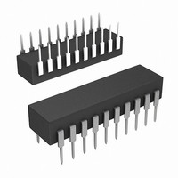
IC CMOS BUS CONTROLLER 20DIP

CP82C88

Manufacturer Part Number
CP82C88
Description
IC CMOS BUS CONTROLLER 20DIP
Manufacturer
Intersil
Datasheet

Specifications of CP82C88

Applications
CMOS Bus Controller
Voltage - Supply
4.5 V ~ 5.5 V
Current - Supply
1mA
Operating Temperature
0°C ~ 70°C
Mounting Type
Through Hole
Package / Case
20-DIP (0.300", 7.62mm)
Operating Supply Voltage (typ)
5V
Operating Supply Voltage (min)
4.5V
Operating Supply Voltage (max)
5.5V
Operating Temp Range
0C to 70C
Operating Temperature Classification
Commercial
Package Type
PDIP
Mounting
Through Hole
Pin Count
20
Lead Free Status / RoHS Status
Contains lead / RoHS non-compliant
Voltage - Input
-
Lead Free Status / Rohs Status
Not Compliant

Available stocks

Company
Part Number
Manufacturer
Quantity
Price
Part Number:
CP82C88
Manufacturer:
RCA
Quantity:
6 219
Part Number:
CP82C88
Manufacturer:
INTERSIL
Quantity:
1 000
Part Number:
CP82C88
Manufacturer:
INTERSIL
Quantity:
20 000
Part Number:
CP82C88Z
Manufacturer:
ST
Quantity:
101
Part Number:
CP82C88Z
Manufacturer:
HARRIS
Quantity:
20 000
CMOS Bus Controller
The Intersil 82C88 is a high performance CMOS Bus
Controller manufactured using a self-aligned silicon gate
CMOS process (Scaled SAJI IV). The 82C88 provides the
control and command timing signals for 80C86, 80C88,
8086, 8088, 8089, 80186, and 80188 based systems. The
high output drive capability of the 82C88 eliminates the need
for additional bus drivers.
Static CMOS circuit design insures low operating power. The
Intersil advanced SAJI process results in performance equal
to or greater than existing equivalent products at a significant
power savings.
Pinouts
AMWC
MRDC
AMWC
MWTC
DT/ R
MRDC
DT/ R
AEN
ALE
GND
AEN
CLK
ALE
IOB
S1
4
5
6
7
8
10
1
2
3
4
5
6
7
8
9
20 LD PDIP, CERDIP
20 LD PLCC, CLCC
3
9
TOP VIEW
TOP VIEW
10
2
®
11
1
1
12
20 19
Data Sheet
13
20
19
18
17
16
15
14
13
12
11
18
17
16
15
14
V
S0
S2
MCE/PDEN
DEN
CEN
INTA
IORC
AIOWC
IOWC
CC
S2
MCE/PDEN
DEN
CEN
INTA
1-888-INTERSIL or 1-888-468-3774
CAUTION: These devices are sensitive to electrostatic discharge; follow proper IC Handling Procedures.
Features
• Compatible with Bipolar 8288
• Performance Compatible with:
• Provides Advanced Commands for Multi-Master Busses
• Three-State Command Outputs
• Bipolar Drive Capability
• Scaled SAJI IV CMOS Process
• Single 5V Power Supply
• Low Power Operation
• Operating Temperature Ranges
• Pb-Free Plus Anneal Available (RoHS Compliant)
Ordering Information
NOTE: Intersil Pb-free plus anneal products employ special Pb-free
material sets; molding compounds/die attach materials and 100%
matte tin plate termination finish, which are RoHS compliant and
compatible with both SnPb and Pb-free soldering operations. Intersil
Pb-free products are MSL classified at Pb-free peak reflow
temperatures that meet or exceed the Pb-free requirements of
IPC/JEDEC J STD-020.
CP82C88
CP82C88Z
(Note)
CP82C88-10 CP82C88-10 20 Ld PDIP
IP82C88
CS82C88
IS82C88
CD82C88
ID82C88
MD82C88/B
8406901RA
MR82C88/B
84069012A
- 80C86/80C88 . . . . . . . . . . . . . . . . . . . . . . . . . (5/8MHz)
- 80186/80188. . . . . . . . . . . . . . . . . . . . . . . . . . (6/8MHz)
- 8086/8088. . . . . . . . . . . . . . . . . . . . . . . . . . . . (5/8MHz)
- 8089
- ICCSB. . . . . . . . . . . . . . . . . . . . . . . . . . . . . .10µA (Max)
- ICCOP . . . . . . . . . . . . . . . . . . . . . . . . . 1mA/MHz (Max)
- C82C88 . . . . . . . . . . . . . . . . . . . . . . . . . . 0°C to +70°C
- I82C88 . . . . . . . . . . . . . . . . . . . . . . . . . . -40°C to +85°C
- M82C88 . . . . . . . . . . . . . . . . . . . . . . . . -55°C to +125°C
NUMBER
PART
August 25, 2005
All other trademarks mentioned are the property of their respective owners.
|
Intersil (and design) is a registered trademark of Intersil Americas Inc.
CP82C88
CP82C88Z
IP82C88
CS82C88
IS82C88
CD82C88
ID82C88
MD82C88/B
8406901RA
MR82C88/B 20 Pad CLCC -55 to +125 J20.A
84069012A
MARKING
Copyright Intersil Americas Inc. 2002, 2005. All Rights Reserved
PART
20 Ld PDIP
20 Ld PDIP
(Pb-free)
20 Ld PLCC
20 Ld
CERDIP
PACKAGE
SMD#
SMD#
-55 to +125 F20.3
-40 to +85 E20.3
-40 to +85 N20.35
-40 to +85 F20.3
RANGE
0 to +70
0 to +70
0 to +70
0 to +70
0 to +70
TEMP
(°C)
82C88
FN2979.2
E20.3
E20.3
E20.3
N20.35
F20.3
F20.3
J20.A
DWG. #
PKG.

Related parts for CP82C88

CP82C88 Summary of contents

Page 1

... M82C88 . . . . . . . . . . . . . . . . . . . . . . . . -55°C to +125°C 16 DEN • Pb-Free Plus Anneal Available (RoHS Compliant) 15 CEN Ordering Information 14 INTA 13 IORC PART NUMBER 12 AIOWC CP82C88 11 IOWC CP82C88Z (Note) CP82C88-10 CP82C88- PDIP IP82C88 CS82C88 IS82C88 18 S2 CD82C88 17 MCE/PDEN ID82C88 16 DEN MD82C88/B 8406901RA 15 CEN MR82C88/B 14 INTA 84069012A NOTE: Intersil Pb-free plus anneal products employ special Pb-free material sets ...

Page 2

Functional Diagram CLK AEN CONTROL INPUT CEN IOB Pin Description PIN SYMBOL NUMBER TYPE The +5V power supply pin. A 0.1µF capacitor between pins 10 and 20 is recommended for decoupling ...

Page 3

Pin Description (Continued) PIN SYMBOL NUMBER TYPE AMWC 8 O ADVANCED MEMORY WRITE COMMAND: The AMWC issues a memory write command earlier in the machine cycle to give memory devices an early indication of a write instruction. Its timing is ...

Page 4

Control Outputs The control outputs of the 82C88 are Data Enable (DEN), Data Transmit/Receive (DT/R) and Master Cascade Enable/ Peripheral Data Enable (MCE/PDEN). The DEN signal determines when the external bus should be enabled onto the local bus and the ...

Page 5

Absolute Maximum Ratings Supply Voltage ...

Page 6

AC Electrical Specifications PARAMETER SYMBOL TIMING REQUIREMENTS (1) TCLCL CLK Cycle Period (2) TCLCH CLK Low Time (3) TCHCL CLK High Time (4) TSVCH Status Active Setup Time (5) TCHSV Status Inactive ...

Page 7

AC Testing Input, Output Waveform INPUT V +0.4V IH 1.5V V -0.4V IL A.C. Testing: All input signals (other than CLK) must switch between V -0.4V and V +0.4. CLK must switch between 0. and V -0.4V. Input ...

Page 8

Timing Waveforms (Note 3) T STATE 4 CLK TCHSV (5) S2, S1, S0 ADDRESS/DATA TCLLH (10) ALE MRDC, IORC, INTA, AMWC, AIOWC MWTC, IOWC DEN (READ) (INTA) PDEN (READ) (INTA) DEN (WRITE) PDEN (WRITE) TCHDTH (18) DT/R (READ) (INTA) MCE ...

Page 9

Timing Waveforms (Note 3) (Continued) CEN AEN DEN PDEN AEN TAELCH (19) OUTPUT COMMAND CEN CEN MUST BE LOW OR INVALID PRIOR PREVENT THE COMMAND FROM BEING GENERATED. FIGURE 3. ADDRESS ENABLE (AEN) TIMING (THREE-STATE ENABLE/DISABLE) NOTES: ...

Page 10

Burn-In Circuits NOTES: = 5.5V ± 0.5V ...

Page 11

... Accordingly, the reader is cautioned to verify that data sheets are current before placing orders. Information furnished by Intersil is believed to be accurate and reliable. However, no responsibility is assumed by Intersil or its subsidiaries for its use; nor for any infringements of patents or other rights of third parties which may result from its use ...

Related keywords