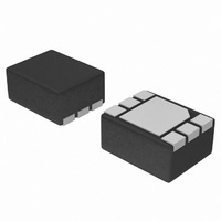
NCP349MNBGTBG ON Semiconductor, NCP349MNBGTBG Datasheet - Page 3

NCP349MNBGTBG
Manufacturer Part Number
NCP349MNBGTBG
Description
IC VOLTAGE DETECTOR OVP 6DFN
Manufacturer
ON Semiconductor
Type
Positive Overvoltage Protection Controllerr
Datasheet
1.NCP349MNBGTBG.pdf
(12 pages)
Specifications of NCP349MNBGTBG
Applications
Overvoltage Protection Controller
Voltage - Supply
1.2 V ~ 28 V
Current - Supply
70µA
Operating Temperature
-40°C ~ 85°C
Mounting Type
Surface Mount
Package / Case
6-VFDFN Exposed Pad
Product
Driver ICs - Various
Supply Voltage (max)
28 V
Supply Voltage (min)
1.2 V
Supply Current
70 uA, 140 uA
Maximum Operating Temperature
+ 85 C
Mounting Style
SMD/SMT
Maximum Turn-off Delay Time
1.5 us
Minimum Operating Temperature
- 40 C
Number Of Drivers
1
Number Of Outputs
1
Lead Free Status / RoHS Status
Lead free / RoHS Compliant
Voltage - Input
-
Lead Free Status / Rohs Status
Lead free / RoHS Compliant
Available stocks
Company
Part Number
Manufacturer
Quantity
Price
Company:
Part Number:
NCP349MNBGTBG
Manufacturer:
ON Semiconductor
Quantity:
30
Stresses exceeding Maximum Ratings may damage the device. Maximum Ratings are stress ratings only. Functional operation above the
Recommended Operating Conditions is not implied. Extended exposure to stresses above the Recommended Operating Conditions may affect
device reliability.
1. The R
2. Human Body Model, 100 pF discharged through a 1.5 kW resistor following specification JESD22/A114.
3. Machine Model, 200 pF discharged through all pins following specification JESD22/A115.
PIN FUNCTION DESCRIPTION
MAXIMUM RATINGS
Pin No.
Minimum Voltage (IN to GND)
Minimum Voltage (All others to GND)
Maximum Voltage (IN to GND)
Maximum Voltage (All others to GND)
Maximum Current (UVLO<V
Maximum Peak Current (t ≤ 1 ms, T
Thermal Resistance, Junction−to−Air (Note 1)
Operating Ambient Temperature Range
Storage Temperature Range
Junction Operating Temperature
ESD Withstand Voltage (IEC 61000−4−2) (input only) when bypassed with 1.0 mF capacitor
Moisture Sensitivity
1, 7
4, 5
Human Body Model (HBM), Model = 2 (Note 2)
Machine Model (MM) Model = B (Note 3)
2
3
6
qJA
Symbol
is highly dependent on the PCB heat sink area (connected to pin 7).
FLAG
GND
OUT
EN
IN
Function
OUTPUT
OUTPUT
POWER
INPUT
INPUT
IN
<OVLO)
A
Fault Indication Pin. This pin allows an external system to detect a fault on the IN pins. The FLAG pin
goes low when input voltage exceeds OVLO threshold or drops below UVLO threshold. Since the
FLAG pin is open drain functionality, an external pull−up resistor to V
10 kW).
Enable Pin. The device enters in shutdown mode when this pin is tied to a high level. In this case the
output is disconnected from the input. To allow normal functionality, the EN pin shall be connected to
GND to a pull down or to a I/O pin. This pin does not have an impact on the fault detection.
Input Voltage Pins. These pins are connected to the Wall Adapoter (AC−DC, Vbus ..). A 1 mF low
ESR ceramic capacitor, or larger, must be connected between these pins and GND, as close as
possible to the DUT. The two IN pins must be connected together to power supply. (See PCB recom-
mendation for the pin7).
Ground
Output Voltage Pins. These pins follow IN pins when “no fault” is detected. The two OUT pins must
be hardwired together.
= 85°C)
Rating
http://onsemi.com
3
Description
Imax
Symbol
Vmax
Vmin
Vmax
Vmin
Imax
Vesd
R
MSL
T
T
T
qJA
stg
A
J
peak
in
in
CC
15 Air, 8.0 Contact
must be added. (Minimum
−65 to +150
−40 to +85
Level 1
Value
2000
−0.3
−0.3
180
150
200
7.0
2.0
4.0
30
°C/W
Unit
°C
°C
°C
kV
V
V
V
V
A
A
V
V
−


