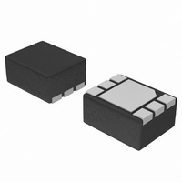
NCP349MNBGTBG ON Semiconductor, NCP349MNBGTBG Datasheet - Page 4

NCP349MNBGTBG
Manufacturer Part Number
NCP349MNBGTBG
Description
IC VOLTAGE DETECTOR OVP 6DFN
Manufacturer
ON Semiconductor
Type
Positive Overvoltage Protection Controllerr
Datasheet
1.NCP349MNBGTBG.pdf
(12 pages)
Specifications of NCP349MNBGTBG
Applications
Overvoltage Protection Controller
Voltage - Supply
1.2 V ~ 28 V
Current - Supply
70µA
Operating Temperature
-40°C ~ 85°C
Mounting Type
Surface Mount
Package / Case
6-VFDFN Exposed Pad
Product
Driver ICs - Various
Supply Voltage (max)
28 V
Supply Voltage (min)
1.2 V
Supply Current
70 uA, 140 uA
Maximum Operating Temperature
+ 85 C
Mounting Style
SMD/SMT
Maximum Turn-off Delay Time
1.5 us
Minimum Operating Temperature
- 40 C
Number Of Drivers
1
Number Of Outputs
1
Lead Free Status / RoHS Status
Lead free / RoHS Compliant
Voltage - Input
-
Lead Free Status / Rohs Status
Lead free / RoHS Compliant
Available stocks
Company
Part Number
Manufacturer
Quantity
Price
Company:
Part Number:
NCP349MNBGTBG
Manufacturer:
ON Semiconductor
Quantity:
30
NOTE:
4. Additional UVLO and OVLO thresholds ranging from UVLO and from OVLO can be manufactured. Contact your ON Semiconductor
ELECTRICAL CHARACTERISTICS
unless otherwise noted.)
TIMINGS
Input Voltage Range
Undervoltage Lockout Threshold (Note 4)
Undervoltage Lockout Hysteresis
Overvoltage Lockout Threshold (Note 4)
Overvoltage Lockout Hysteresis
V
Supply Quiescent Current
UVLO Supply Current
FLAG Output Low Voltage
FLAG Leakage Current
EN Voltage High
EN Voltage Low
EN Leakage Current
Startup Delay
FLAG Going Up Delay
Output Turn Off Time
Alert Delay
Disable Time
in
representative for availability.
NCP349MN, NCP349MNAE, NCP349MNBG
versus V
Electrical parameters are guaranteed by correlation across the full range of temperature.
out
Resistance
Characteristic
NCP349MNBG, NCP349MNBK
NCP349MNBG, NCP349MNBK
NCP349MNBG, NCP349MNBK
NCP349MN, NCP349MNAE
NCP349MNBG
NCP349MNAE
NCP349MNBK
NCP349MNBK
NCP349MNAE
NCP349MNAE
NCP349MN
NCP349MN
NCP349MN
(Min/Max limits values (−40°C < T
UVLO
OVLO
FLAG
Symbol
R
Idd
EN
OVLO
UVLO
Vol
tstart
tstop
DS(on)
tdis
V
Idd
Vih
Vol
ton
toff
uvlo
leak
in
flag
leak
hyst
hyst
http://onsemi.com
From V
V
From V
V
V
V
From V
V
in
V
From V
in
in
in
in
in
rises above UVLO + UVLO
4
0.4 V (See Figures 4 & 10)
falls below OVLO + OVLO
increasing from 5.0 V to 8.0 V
increasing from 5.0 V to 8.0 V
Sink 1.0 mA on FLAG pin
rises above OVLO threshold
Rload connected on V
Rload connected on V
Sink 50 mA on/FLAG pin
falls below UVLO threshold
V
Load connected to V
From EN > = 1.2 V to
(See Figures 5 & 12)
in
No load. EN = 5.0 V
1.2 V < V
out
in
EN = 5.0 V or GND
(See Figures 3 & 7)
(See Figures 3 & 9)
(See Figures 4 & 8)
No load. EN = Gnd
FLAG level = 5.0 V
in
from 5 V to 2.7 V
= 5.0 V, EN = GND,
> OVLO to V
in
Rload = 5.0 W
> UVLO to V
= 0.3 V to FLAG = 1.2 V
A
V
Conditions
> OVLO to FLAG < =
V
V
at 3.0 V/ms
at 3.0 V/ms
< +85°C) and V
IN
out
IN
> OVLO
= 2.7 V
< 0.3 V
−
IN
−
−
< UVLO
out
out
< = 0.3 V
out
= 0.3 V
out
out
in
= +5.0 V. Typical values are T
hyst
hyst
5.53
5.70
6.67
Min
1.2
2.8
3.0
6.0
1.2
1.0
6.0
0.4
6.0
30
30
50
30
30
−
−
−
−
−
−
−
−
−
−
−
−
2.95
3.25
5.68
6.02
6.85
Typ
100
140
6.4
1.0
1.0
1.8
1.2
1.5
1.0
1.0
60
60
65
70
60
20
10
55
10
55
−
−
−
−
Max
5.83
6.40
7.05
150
150
250
400
400
110
A
3.1
3.5
6.8
0.4
2.7
2.1
5.0
5.0
28
90
90
14
70
14
70
−
−
−
−
−
= +25°C,
Unit
mW
mV
mV
mV
mV
ms
ms
mA
mA
mA
nA
nA
ms
ms
ms
V
V
V
V
V


