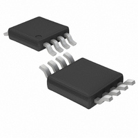
LTC1966CMS8 Linear Technology, LTC1966CMS8 Datasheet - Page 21

LTC1966CMS8
Manufacturer Part Number
LTC1966CMS8
Description
IC PREC RMS/DC CONV MCRPWR 8MSOP
Manufacturer
Linear Technology
Datasheet
1.LTC1966CMS8.pdf
(32 pages)
Specifications of LTC1966CMS8
Current - Supply
155µA
Voltage - Supply
2.7 V ~ 5.5 V
Mounting Type
Surface Mount
Package / Case
8-MSOP, Micro8™, 8-uMAX, 8-uSOP,
Lead Free Status / RoHS Status
Contains lead / RoHS non-compliant
Available stocks
Company
Part Number
Manufacturer
Quantity
Price
Part Number:
LTC1966CMS8
Manufacturer:
LINEAR/凌特
Quantity:
20 000
Company:
Part Number:
LTC1966CMS8#PBF/H/MP
Manufacturer:
LT
Quantity:
2 335
APPLICATIO S I FOR ATIO
frequency. So with AC + DC waveforms, the required
value for C
frequency, using the same design curves presented in
Figures 6, 8, 17 and 18.
Crest factor, which is the peak to RMS ratio of a dynamic
signal, also effects the required C
crest factor, more of the energy in the signal is concentrated
into a smaller portion of the waveform, and the averaging
has to ride out the long lull in signal activity. For busy
waveforms, such as a sum of sine waves, ECG traces or
SCR-chopped sine waves, the required value for C
should be based on the lowest fundamental input frequency
divided as such:
f
0.1
0.1
10
DESIGN
10
1
0.01
1
0.01
AVE
3
should be based on half of the lowest input
f
•
INPUT MIN
CF
U
C = 0.1 F
(
–
C = 0.1 F
U
)
2
C = 0.22 F
C = 0.22 F
0.1
0.1
AVE
W
Figure 20. Settling Time with DC-Accurate Post Filter
value. With a higher
Figure 19. Settling Time with Buffered Post Filter
C = 0.47 F
C = 0.47 F
U
C = 1.0 F
C = 1.0 F
AVE
SETTLING TIME (SEC)
SETTLING TIME (SEC)
C = 2.2 F
C = 2.2 F
1
1
using the same design curves presented in Figures 6, 8,
17 and 18. For the worst case of square top pulse trains,
that are always either zero volts or the peak voltage, base
the selection on the lowest fundamental input frequency
divided by twice as much:
The effects of crest factor and DC offsets are cumulative.
So for example, a 10% duty cycle pulse train from 0V
to 1V
input is effectively only 30Hz due to the DC asymmetry and
is effectively only:
for the purposes of Figures 6, 8, 17 and 18.
f
f
DESIGN
DESIGN
PEAK
C = 4.7 F
C = 4.7 F
(CF = 10 = 3.16) repeating at 16.67ms (60Hz)
6
6
C = 10 F
f
•
•
INPUT MIN
C = 10 F
CF
3 16
.
30
(
–
–
C = 22 F
C = 22 F
)
2
10
10
2
3 78
C = 47 F
.
C = 47 F
Hz
LTC1966
C = 100 F
C = 100 F
sn1966 1966fas
21
1066 F14
1066 F20
PEAK
100
100


