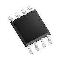
MCP9804-E/MS Microchip Technology, MCP9804-E/MS Datasheet - Page 11

MCP9804-E/MS
Manufacturer Part Number
MCP9804-E/MS
Description
IC TEMP SENSOR I2C 2.7V 8MSOP
Manufacturer
Microchip Technology
Specifications of MCP9804-E/MS
Package / Case
8-MSOP, Micro8™, 8-uMAX, 8-uSOP,
Function
Temp Monitoring System (Sensor)
Topology
ADC (Sigma Delta), Register Bank
Sensor Type
Internal
Sensing Temperature
-40°C ~ 125°C
Output Type
I²C™/SMBus™
Output Alarm
No
Output Fan
No
Voltage - Supply
2.7 V ~ 5.5 V
Operating Temperature
-40°C ~ 125°C
Mounting Type
Surface Mount
Temperature Threshold
+ 150 C
Full Temp Accuracy
+/- 0.25 %
Digital Output - Bus Interface
2-Wire, I2C
Supply Voltage (max)
5.5 V
Supply Voltage (min)
2.7 V
Maximum Operating Temperature
+ 125 C
Minimum Operating Temperature
- 40 C
Supply Current
200 uA
Ic Output Type
Digital
Sensing Accuracy Range
± 0.25°C
Temperature Sensing Range
-40°C To +125°C
Supply Voltage Range
2.7V To 5.5V
Sensor Case Style
MSOP
No. Of Pins
8
Rohs Compliant
Yes
Supply Voltage Min
2.7V
Leaded Process Compatible
Yes
Lead Free Status / RoHS Status
Lead free / RoHS Compliant
Lead Free Status / RoHS Status
Lead free / RoHS Compliant, Lead free / RoHS Compliant
Available stocks
Company
Part Number
Manufacturer
Quantity
Price
Company:
Part Number:
MCP9804-E/MS
Manufacturer:
MICROCHIP
Quantity:
12 000
Part Number:
MCP9804-E/MS
Manufacturer:
MICROCHI
Quantity:
20 000
3.0
The descriptions of the pins are listed in
TABLE 3-1:
3.1
These pins are device address input pins.
The address pins correspond to the Least Significant
bits (LSb) of address bits. The Most Significant bits
(MSb) (A6, A5, A4, A3). This is shown in
TABLE 3-2:
3.2
The GND pin is the system ground pin.
3.3
SDA is a bidirectional input/output pin, used to serially
transmit data to/from the host controller. This pin
requires a pull-up resistor. (See Section 4.0).
© 2009 Microchip Technology Inc.
MCP9804
MCP9804
Note 1: User-selectable address is shown by X.
Device
DFN
1
2
3
4
5
6
7
8
9
2: Contact Factory for this Address Code.
PIN DESCRIPTION
Address Pins (A0, A1, A2)
Ground Pin (GND)
Serial Data Line (SDA)
(2)
A2, A1 and A0 must match the
corresponding device pin configuration.
PIN FUNCTION TABLE
MCP9804 ADDRESS BYTE
A6
0
1
MSOP
Address Code
—
1
2
3
4
5
6
7
8
A5
0
0
A4
1
0
A3
1
1
Symbol
GND
SDA
SCL
Alert
V
X
EP
A2
A1
A0
A2
DD
X
Table
(1)
Table
Address
Slave
A1
X
X
3-1.
3-2.
A0
X
X
Serial Data Line
Serial Clock Line
Temperature Alert Output
Ground
Slave Address
Slave Address
Slave Address
Power Pin
Exposed Thermal Pad (EP); must be connected to GND.
3.4
The SCL is a clock input pin. All communication and
timing is relative to the signal on this pin. The clock is
generated by the host or master controller on the bus.
(See Section 4.0).
3.5
The MCP9804 temperature alert output pin is an
open-drain output. The device outputs a signal when
the
user-programmed
Section 5.2.3).
3.6
V
specified in the DC electrical specification table, is
applied on this pin.
3.7
There is an internal electrical connection between the
Exposed Thermal Pad (EP) and the GND pin. The EP
may be connected to the system ground on the Printed
Circuit Board (PCB).
DD
is the power pin. The operating voltage range, as
ambient
Serial Clock Line (SCL)
Temperature Alert, Open-Drain
Output (Alert)
Power Pin (V
Exposed Thermal Pad (EP)
Pin Function
temperature
temperature
DD
)
MCP9804
goes
DS22203B-page 11
limit.
beyond
(See
the


