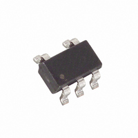
DS1775R1+T&R Maxim Integrated Products, DS1775R1+T&R Datasheet - Page 10

DS1775R1+T&R
Manufacturer Part Number
DS1775R1+T&R
Description
IC THERMOM/STAT DIG 001 SOT-23-5
Manufacturer
Maxim Integrated Products
Datasheet
1.DS1775RTR.pdf
(14 pages)
Specifications of DS1775R1+T&R
Function
Thermometer, Thermostat
Topology
ADC, Comparator, Register Bank
Sensor Type
Internal
Sensing Temperature
-55°C ~ 125°C
Output Type
I²C™/SMBus™
Output Alarm
Yes
Output Fan
No
Voltage - Supply
2.7 V ~ 5.5 V
Operating Temperature
-55°C ~ 125°C
Mounting Type
Surface Mount
Package / Case
SOT-23-5, SC-74A, SOT-25
Full Temp Accuracy
+/- 3 C
Digital Output - Bus Interface
Serial (2-Wire)
Digital Output - Number Of Bits
12 bit
Maximum Operating Temperature
+ 125 C
Minimum Operating Temperature
- 55 C
Lead Free Status / RoHS Status
Lead free / RoHS Compliant
DATA TRANSFER ON 2–WIRE SERIAL BUS Figure 4
Figure 5 details how data transfer is accomplished on the two–wire bus. Depending upon the state of the
R/W bit, two types of data transfer are possible:
1. Data transfer from a master transmitter to a slave receiver. The first byte transmitted by the
2. Data transfer from a slave transmitter to a master receiver. The first byte (the slave address) is
The master device generates all of the serial clock pulses and the START and STOP conditions. A
transfer is ended with a STOP condition or with a repeated START condition. Since a repeated START
condition is also the beginning of the next serial transfer, the bus will not be released.
The DS1775 may operate in the following two modes:
1. Slave receiver mode: Serial data and clock are received through SDA and SCL. After each byte is
2. Slave transmitter mode: The first byte is received and handled as in the slave receiver mode.
SLAVE ADDRESS
A control byte is the first byte received following the START condition from the master device. The
control byte consists of a four bit control code; for the DS1775, this is set as 1001 binary for read and
write operations. The next three bits of the control byte are the device select bits (A2, A1, A0). These bits
are set to 000 (A2="0", A1="0", A0="0") for the DS1775R/TRL and vary according to the device's part
number as specified in the "Ordering Information" section. They are used by the master device to select
which of eight devices are to be accessed. The set bits are in effect the three least significant bits of the
slave address. The last bit of the control byte (R/
"1" a read operation is selected, and when set to a "0" a write operation is selected. Following the START
condition, the DS1775 monitors the SDA bus checking the device type identifier being transmitted. Upon
receiving the 1001 code and appropriate device select bits of 000, the DS1775 outputs an acknowledge
signal on the SDA line.
master is the slave address. Next follows a number of data bytes. The slave returns an acknowledge
bit after each received byte.
transmitted by the master. The slave then returns an acknowledge bit. Next follows a number of data
bytes transmitted by the slave to the master. The master returns an acknowledge bit after all received
bytes other than the last byte. At the end of the last received byte, a ‘not acknowledge’ is returned.
received, an acknowledge bit is transmitted. START and STOP conditions are recognized as the
beginning and end of a serial transfer. Address recognition is performed by hardware after reception
of the slave address and direction bit.
However, in this mode, the direction bit will indicate that the transfer direction is reversed. Serial data
is transmitted on SDA by the DS1775 while the serial clock is input on SCL. START and STOP
conditions are recognized as the beginning and end of a serial transfer.
W
10 of 14
) defines the operation to be performed. When set to a


