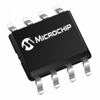
TCN75-3.3MUAG Microchip Technology, TCN75-3.3MUAG Datasheet - Page 7

TCN75-3.3MUAG
Manufacturer Part Number
TCN75-3.3MUAG
Description
IC TEMP SENSOR SRL 3.3V 8MSOP
Manufacturer
Microchip Technology
Specifications of TCN75-3.3MUAG
Function
Temp Monitoring System (Sensor)
Topology
ADC (Sigma Delta), Register Bank
Sensor Type
Internal
Sensing Temperature
-55°C ~ 125°C
Output Type
2-Wire Serial
Output Alarm
Yes
Output Fan
No
Voltage - Supply
2.7 V ~ 5.5 V
Operating Temperature
-55°C ~ 125°C
Mounting Type
Surface Mount
Package / Case
8-MSOP, Micro8™, 8-uMAX, 8-uSOP,
Temperature Threshold
Programmable
Full Temp Accuracy
3 C
Digital Output - Bus Interface
2-Wire
Digital Output - Number Of Bits
9 bit
Supply Voltage (max)
5.5 V
Supply Voltage (min)
2.7 V
Description/function
2-Wire Serial Input/Output - Thermal Monitors
Maximum Operating Temperature
+ 125 C
Minimum Operating Temperature
- 55 C
Supply Current
1 mA
Lead Free Status / RoHS Status
Lead free / RoHS Compliant
systems. The INT/CMPTR output may be wire-OR'ed
with other interrupt sources in such systems. Note that
a pull-up resistor is necessary on this pin since it is an
open-drain output. Entering Shutdown mode will
unconditionally RESET INT/CMPTR when in Interrupt
mode.
4.0
When the appropriate bit is set in the configuration reg-
ister (CONFIG) the TCN75 enters its low power Shut-
down mode (I
to-digital conversion process is halted. The TCN75's
bus interface remains active and TEMP, T
T
SDA or SCL due to external bus activity may increase
the standby power consumption. If the TCN75 is in
Interrupt mode, the state of INT/CMPTR will be RESET
upon entering Shutdown mode.
4.1
To lessen the probability of spurious activation of INT/
CMPTR the TCN75 may be programmed to filter out
transient events. This is done by programming the
desired value into the Fault Queue. Logic inside the
TCN75 will prevent the device from triggering INT/
CMPTR unless the programmed number of sequential
temperature-to-digital conversions yield the same
qualitative result. In other words, the value reported in
TEMP must remain above T
consecutive number of cycles programmed in the Fault
Queue. Up to a six-cycle "filter" may be selected. See
Section 5.0, Register Set and Programmer's Model.
4.2
The Serial Clock input (SCL) and bi-directional data
port (SDA) form a 2-wire bi-directional serial port for
programming and interrogating the TCN75. The
following table indicates TCN75 conventions that are
used in this bus scheme.
©
HYST
2002 Microchip Technology Inc.
may be read from and written to. Transitions on
SHUTDOWN MODE
Fault Queue
Serial Port Operation
DD
= 1µA, typical) and the temperature-
SET
or below T
HYST
SET
for the
, and
TABLE 4-1:
All transfers take place under control of a host, usually
a CPU or microcontroller, acting as the Master, which
provides the clock signal for all transfers. The TCN75
always operates as a Slave. This serial protocol is
illustrated in Figure 5-1. All data transfers have two
phases; and all bytes are transferred MSB first.
Accesses are initiated by a START condition, followed
by a device address byte and one or more data bytes.
The device address byte includes a Read/Write
selection bit. Each access must be terminated by a
STOP condition. A convention called Acknowledge
(ACK) confirms receipt of each byte. Note that SDA can
change only during periods when SCL is LOW (SDA
changes while SCL is HIGH are reserved for START
and STOP conditions).
4.3
The TCN75 continuously monitors the SDA and SCL
lines for a START condition (a HIGH to LOW transition
of SDA while SCL is HIGH), and will not respond until
this condition is met.
Transmitter
NOT Busy
Data Valid
Receiver
START
Master
STOP
Slave
Term
ACK
START Condition (START)
The device sending data to the bus.
The device receiving data from the bus.
The device which controls the bus: initiating
transfers (START), generating the clock, and
terminating transfers (STOP).
The device addressed by the master.
A unique condition signaling the beginning of
a transfer indicated by SDA falling (High-
Low) while SCL is high.
A unique condition signaling the end of a
transfer indicated by SDA rising (Low - High)
while SCL is high.
A Receiver acknowledges the receipt of each
byte with this unique condition. The Receiver
drives SDA low during SCL high of the ACK
clock-pulse. The Master provides the clock
pulse for the ACK cycle.
When the bus is idle, both SDA & SCL will
remain high.
The state of SDA must remain stable during
the High period of SCL in order for a data bit
to be considered valid. SDA only changes
state while SCL is low during normal data
transfers. (See START and STOP condi-
tions).
SERIAL BUS CONVENTIONS
Explanation
TCN75
DS21490B-page 7


