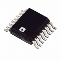
ADT7517ARQ Analog Devices Inc, ADT7517ARQ Datasheet - Page 29

ADT7517ARQ
Manufacturer Part Number
ADT7517ARQ
Description
IC TEMP SNSR QUAD DAC 16-QSOP
Manufacturer
Analog Devices Inc
Datasheet
1.ADT7517ARQZ.pdf
(44 pages)
Specifications of ADT7517ARQ
Rohs Status
RoHS non-compliant
Function
Temp Monitoring System (Sensor)
Topology
ADC, Comparator, Multiplexer, Register Bank
Sensor Type
External & Internal
Sensing Temperature
-40°C ~ 120°C, External Sensor
Output Type
I²C™, MICROWIRE™, QSPI™, SPI™
Output Alarm
No
Output Fan
No
Voltage - Supply
2.7 V ~ 5.5 V
Operating Temperature
-40°C ~ 120°C
Mounting Type
Surface Mount
Package / Case
16-QSOP
Available stocks
Company
Part Number
Manufacturer
Quantity
Price
Company:
Part Number:
ADT7517ARQZ
Manufacturer:
Analog Devices Inc
Quantity:
135
R/W
Address
0x14
0x15
0x16
0x17
0x18
0x19
0x1A
0x1B
0x1C
0x1D
0x1E
0x1F
0x20
0x21
0x22
0x23
0x24
0x25
0x26
0x27
0x28
0x29 to
0x2A
0x2B
0x2C
0x2D
0x2E
0x2F
0x30
0x31 to
0x4C
0x4D
0x4E
0x4F
0x50 to
0x7E
0x7F
0x80 to
0xFF
Interrupt Status 1 Register (Read-Only) [Address 0x00]
This 8-bit read-only register reflects the status of some of the
interrupts that can cause the INT/ INT pin to go active. This
register is reset by a read operation, provided that any out-of-
limit event has been corrected. It is also reset by a software reset.
D7
0
1
Default settings at power-up.
1
D6
0
1
Name
DAC C LSBs (ADT7516/ADT7517 only)
DAC C MSBs
DAC D LSBs (ADT7516/ADT7517 only)
DAC D MSBs
Control Configuration 1
Control Configuration 2
Control Configuration 3
DAC Configuration
LDAC Configuration
Interrupt Mask 1
Interrupt Mask 2
Internal Temp Offset
External Temp Offset
Internal Analog Temp Offset
External Analog Temp Offset
V
V
Internal T
Internal T
External T
External T
Reserved
AIN2 V
AIN2 V
AIN3 V
AIN3 V
AIN4 V
AIN4 V
Reserved
Device ID
Manufacturer’s ID
Silicon Revision
Reserved
SPI Lock Status
Reserved
DD
DD
V
V
HIGH
LOW
D5
0
1
HIGH
LOW
HIGH
LOW
HIGH
LOW
Limit
Limit
HIGH
LOW
HIGH
LOW
Limit
Limit
Limit
Limit
Limit
Limit
Limit
/AIN1 V
Limit
/AIN1 V
D4
0
1
LOW
HIGH
D3
0
Limits
1
Limits
D2
0
1
D1
0
0xFF
0xFF
0xFF
Power-On
Default
0x00
0x00
0x00
0x00
0x00
0x00
0x00
0x00
0x00
0x00
0x00
0x00
0x00
0xD8
0xD8
0xC7
0x62
0x64
0xC9
0xFF
0x00
0x 00
0x00
0x00
0x03/0x0B/0x07
0x41
Check register
for current
silicon revision
0x00
0x00
0x00
1
D0
0
1
Rev. B | Page 29 of 44
Table 11.
Bit
D0
D1
D2
D3
D4
D5
D6
D7
Interrupt Status 2 Register (Read-Only) [Address = 0x01]
This 8-bit read-only register reflects the status of the V
interrupt that can cause the INT/ INT pin to go active. This
register is reset by a read operation, provided that any out-of-
limit event has been corrected. It is also reset by a software reset.
D7
N/A
1
Table 12.
Bit
D4
Internal Temperature Value/V
(Read-Only) [Address = 0x03]
This 8-bit read-only register stores the two LSBs of the 10-bit
temperature reading from the internal temperature sensor and
the two LSBs of the 10-bit supply voltage reading.
D7
N/A
N/A
1
Default settings at power-up.
Default settings at power-up.
Function
1 when the internal temperature value exceeds T
Any internal temperature reading greater than the set limit
causes an out-of-limit event.
1 when internal temperature value exceeds T
internal temperature reading less than or equal to the set
limit causes an out-of-limit event.
This status bit is linked to the configuration of Pin 7 and
Pin 8. If configured for external temperature sensor, this bit
is 1 when the external temperature value exceeds T
limit. The default value for this limit register is –1°C, so any
external temperature reading greater than the set limit
causes an out-of-limit event. If configured for AIN1 and
AIN2, this bit is 1 when AIN1 input voltage exceeds V
V
1 when external temperature value exceeds T
default value for this limit register is 0°C, so any external
temperature reading less than or equal to the set limit
causes an out-of-limit event.
1 indicates a fault (open or short) for the external
temperature sensor.
1 when AIN2 voltage is greater than its corresponding V
limit. 1 when AIN2 voltage is less than or equal to its
corresponding V
1 when AIN3 voltage is greater than its corresponding V
limit. 1 when AIN3 voltage is less than or equal to its
corresponding V
1 when AIN4 voltage is greater than its corresponding V
limit. 1 when AIN4 voltage is less than or equal to its
corresponding V
Function
1 when V
limit. 1 when V
V
LOW
LOW
D6
N/A
D6
N/A
N/A
limits.
limit.
DD
D5
N/A
value is greater than its corresponding V
D5
N/A
N/A
ADT7516/ADT7517/ADT7519
DD
LOW
LOW
LOW
is less than or equal to its corresponding
limit.
limit.
limit.
D4
0
D4
N/A
N/A
1
D3
N/A
DD
D3
V1
0
1
Value Register LSBs
D2
N/A
D2
LSB
0
1
D1
N/A
LOW
LOW
D1
T1
0
1
limit. Any
HIGH
limit. The
DD
HIGH
HIGH
HIGH
limit.
D0
N/A
D0
LSB
0
or
1
HIGH
HIGH
HIGH


