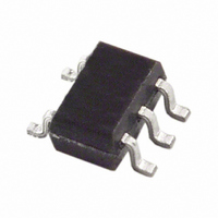
TMP05AKS-REEL Analog Devices Inc, TMP05AKS-REEL Datasheet - Page 6

TMP05AKS-REEL
Manufacturer Part Number
TMP05AKS-REEL
Description
IC SENSOR TEMP PWM OUT SC70-5
Manufacturer
Analog Devices Inc
Datasheet
1.TMP05ARTZ-500RL7.pdf
(28 pages)
Specifications of TMP05AKS-REEL
Function
Temp Monitoring System (Sensor)
Topology
ADC (Sigma Delta), Averaging Control
Sensor Type
Internal
Sensing Temperature
-40°C ~ 150°C
Output Type
CMOS/TTL
Output Alarm
No
Output Fan
No
Voltage - Supply
3 V ~ 5.5 V
Operating Temperature
-40°C ~ 150°C
Mounting Type
Surface Mount
Package / Case
SC-70-5, SC-88A, SOT-323-5, SOT-353, 5-TSSOP
Lead Free Status / RoHS Status
Contains lead / RoHS non-compliant
TMP05/TMP06
Parameter
TMP05 OUTPUT (PUSH-PULL)
TMP06 OUTPUT (OPEN DRAIN)
DIGITAL INPUTS
1
2
3
4
5
6
7
The accuracy specifications for 3.0 V to 3.6 V and 4.5 V to 5.5 V supply ranges are specified to 3-Σ performance.
It is not recommended to operate the device at temperatures above 125°C for more than a total of 5% (5,000 hours) of the lifetime of the device. Any exposure beyond
this limit affects device reliability.
Normal mode current relates to current during T
Guaranteed by design and characterization, not production tested.
It is advisable to restrict the current being pulled from the TMP05 output because any excess currents going through the die cause self-heating. As a consequence,
false temperature readings can occur.
Test load circuit is 100 pF to GND.
Test load circuit is 100 pF to GND, 10 kΩ to 5.5 V.
Power Dissipation
Output High Voltage (V
Output Low Voltage (V
Output High Current (I
Pin Capacitance
Rise Time (t
Fall Time (t
R
Output Low Voltage (V
Output Low Voltage (V
Pin Capacitance
High Output Leakage Current (I
Device Turn-On Time
Fall Time (t
R
Input Current
Input Low Voltage (V
Input High Voltage (V
Pin Capacitance
ON
ON
1 SPS
Resistance (Low Output)
Resistance (Low Output)
HL
HL
LH
)
)
)
6
7
4
6
IL
IH
)
OUT
OL
OL
OL
)
OH
)
)
)
)
)
5
4
4
OH
)
L
. TMP05/TMP06 are not converting during T
Min
V
2
0.7 × V
3
DD
− 0.3
DD
Rev. B | Page 6 of 28
Typ
803.33
101.9
186.9
10
50
50
55
10
0.1
20
30
55
Max
0.4
0.4
1.2
5
±1
0.3 × V
10
H
, so quiescent current relates to current during T
DD
Unit
μW
μW
μW
V
V
mA
pF
ns
ns
Ω
V
V
pF
μA
ms
ns
Ω
μA
V
V
pF
Test Conditions/Comments
V
nominal conversion rates @ 25°C
Average power dissipated for V
one shot mode @ 25°C
Average power dissipated for V
one shot mode @ 25°C
I
I
Typical V
Supply and temperature dependent
I
I
PWM
Supply and temperature dependent
V
OH
OL
OL
OL
DD
IN
= 800 μA
= 1.6 mA
= 5.0 mA
= 800 μA
= 0 V to V
= 3.3 V, continuously converting at
OUT
= 5.5 V
OH
= 3.17 V with V
DD
H
.
DD
= 3.3 V
DD
DD
= 3.3 V,
= 5.0 V,


