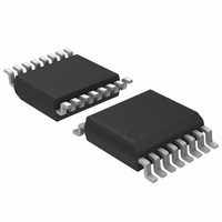
ADT7483AARQZ-REEL7 ON Semiconductor, ADT7483AARQZ-REEL7 Datasheet - Page 15

ADT7483AARQZ-REEL7
Manufacturer Part Number
ADT7483AARQZ-REEL7
Description
IC TEMP SENSOR/ALARM 3CH 16-QSOP
Manufacturer
ON Semiconductor
Datasheet
1.ADT7483AARQZ.pdf
(24 pages)
Specifications of ADT7483AARQZ-REEL7
Function
Temp Monitoring System (Sensor)
Topology
ADC, Comparator, Multiplexer, Register Bank
Sensor Type
External & Internal
Sensing Temperature
-40°C ~ 125°C, External Sensor
Output Type
SMBus™
Output Alarm
Yes
Output Fan
Yes
Voltage - Supply
3 V ~ 3.6 V
Operating Temperature
-40°C ~ 125°C
Mounting Type
Surface Mount
Package / Case
16-QSOP
Lead Free Status / RoHS Status
Lead free / RoHS Compliant
The value in the offset register is added or subtracted to the
measured value of the remote temperature.
The offset register powers up with a default value of 0°C and
will have no effect unless the user writes a different value to it.
Table 13. Sample Offset Register Codes
Offset Value
−128°C
−4°C
−1°C
−0.25°C
0°C
+0.25°C
+1°C
+4°C
+127.75°C
One-Shot Register
The one-shot register is used to initiate a conversion and
comparison cycle when the ADT7483A is in standby mode,
after which the device returns to standby. Writing to the one-
shot register address (0x0F) causes the ADT7483A to perform
a conversion and comparison on both the local and the remote
temperature channels. This is not a data register as such, and it
is the write operation to Address 0x0F that causes the one-shot
0x11/0x34
1000 0000
1111 1100
1111 1111
1111 1111
0000 0000
0000 0000
0000 0001
0000 0100
0111 1111
0x12/0x35
00 00 0000
00 00 0000
00 000000
10 00 0000
00 00 0000
01 00 0000
00 00 0000
00 00 0000
11 00 0000
Rev. 1 | Page 15 of 24 | www.onsemi.com
conversion. The data written to this address is irrelevant and is
not stored.
Consecutive ALERT Register
The value written to this register determines how many out-of-
limit measurements must occur before an ALERT is generated.
The default value is that one out-of-limit measurement generates
an ALERT. The maximum value that can be chosen is 4. The
purpose of this register is to allow the user to perform some
filtering of the output. This is particularly useful at the fastest
three conversion rates, where no averaging takes place. This
register is at Address 0x22.
Table 14. Consecutive ALERT Register Bit
Register
Value
yzax 000x
yzax 001x
yzax 011x
yzax 111x
x = don’t care bit.
y = SMBus SCL timeout bit. Default = 0. See the SMBus section for more
z = SMBus SDA timeout bit. Default = 0. See the SMBus section for more
a = mask internal ALERT s
information.
information.
Number of Out-of-Limit
Measurements Required
1
2
3
4
ADT7483A


