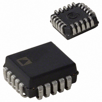
AD652JP-REEL7 Analog Devices Inc, AD652JP-REEL7 Datasheet - Page 3

AD652JP-REEL7
Manufacturer Part Number
AD652JP-REEL7
Description
IC V-F CONV SYNCH MONO 5V 20PLCC
Manufacturer
Analog Devices Inc
Type
Voltage to Frequencyr
Datasheet
1.AD652JPZ.pdf
(28 pages)
Specifications of AD652JP-REEL7
Rohs Status
RoHS non-compliant
Frequency - Max
2MHz
Full Scale
±25ppm/°C
Linearity
±0.005%
Mounting Type
Surface Mount
Package / Case
20-LCC (J-Lead)
Converter Function
VFC
Full Scale Frequency
2000
Power Supply Requirement
Single/Dual
Single Supply Voltage (max)
36V
Single Supply Voltage (min)
12V
Dual Supply Voltage (typ)
±15V
Dual Supply Voltage (min)
±6V
Dual Supply Voltage (max)
±18V
Operating Temperature (min)
0C
Operating Temperature (max)
70C
Operating Temperature Classification
Commercial
Package Type
PLCC
Lead Free Status / Rohs Status
Not Compliant
Available stocks
Company
Part Number
Manufacturer
Quantity
Price
Company:
Part Number:
AD652JP-REEL7
Manufacturer:
Analog Devices Inc
Quantity:
10 000
SPECIFICATIONS
Typical @ T
outgoing quality levels.
Table 1.
Parameter
VOLTAGE-TO-FREQUENCY MODE
FREQUENCY-TO-VOLTAGE MODE
INPUT RESISTORS
INTEGRATOR OP AMP
Gain Error
Gain Temperature Coefficient
Power Supply Rejection Ratio
Linearity Error
Offset (Transfer Function, RTI)
Offset Temperature Coefficient
Response Time
CERDIP (Figure 2)(0 to 10 V FS Range)
PLCC (Figure 3)
Temperature Coefficient (All)
Input Bias Current
Input Offset Current
Input Offset Current Drift
Input Offset Voltage
Input Offset Voltage Drift
Open-Loop Gain
Common-Mode Input Range
CMRR
Bandwidth
Output Voltage Range
f
f
f
f
f
f
f
f
f
f
Gain Error, f
Linearity Error, f
Pin 8 to Pin 7
Pin 7 to Pin 5 (0 V to 5 V FS Range)
Pin 8 to Pin 5 (0 V to 10 V FS Range)
Pin 9 to Pin 5 (0 V to 8 V FS Range)
Pin 10 to Pin 5 (Auxiliary Input)
Inverting Input (Pin 5)
Noninverting Input (Pin 6)
(Referred to Pin 6, R1 > = 5 kΩ)
CLOCK
CLOCK
CLOCK
CLOCK
CLOCK
CLOCK
CLOCK
CLOCK
CLOCK
CLOCK
= 200 kHz
= 1 MHz
= 4 MHz
= 200 kHz
= 1 MHz
= 4 MHz
= 200 kHz
= 1 MHz
= 2 MHz
= 4 MHz
A
= 25°C, V
IN
= 100 kHz FS
IN
= 100 kHz FS
S
= ±15 V, unless otherwise noted. Specifications in boldface are 100% tested at final test and are used to measure
Min
19.8
9.9
9.9
19.8
15.8
19.8
–V
80
14
−1
S
Rev. C | Page 3 of 28
One Period of New Output Frequency Plus One Clock Period.
+ 5
AD652JP/AQ/SQ
Typ
±0.5
±0.5
±0.5
±25
±25
±10
±25
0.001
±0.002
±0.002
±0.01
±0.02
± 1
±10
±0.5
±0.002
20
10
10
20
16
20
±50
±5
20
20
1
±1
±10
86
95
Max
±1
±1
±1.5
±50
±50
±50
±75
0.01
±0.02
±0.02
±0.02
±0.05
±3
±50
±1
±0.02
20.2
10.1
10.1
20.2
16.2
20.2
±100
±20
50
70
3
±3
±25
+V
(+V
S
S
– 5
− 4)
Min
19.8
9.9
9.9
19.8
15.8
19.8
–V
80
−1
S
+ 5
AD652KP/BQ
Typ
±0.25
±0.25
±0.25
±15
±15
±10
±15
0.001
±0.002
±0.002
±0.002
±0.01
±1
±10
±0.25
±0.002
20
10
10
20
16
20
±50
±5
20
20
1
±1
±10
86
14
Max
±0.5
±0.5
±0.75
±25
±25
±30
±50
0.01
±0.005
±0.005
±0.005
±0.02
±2
±25
±0.5
±0.01
20.2
10.1
10.1
20.2
16.2
20.2
±100
±20
50
70
2
±2
±15
+V
95
(+V
S
S
– 5
− 4)
Unit
%
%
%
ppm/°C
ppm/°C
ppm/°C
ppm/°C
%/V
%
%
%
%
mV
µV/°C
%
%
kΩ
kΩ
kΩ
kΩ
kΩ
kΩ
ppm/°C
nA
nA
nA
nA/°C
mV
µV/°C
dB
V
dB
MHz
V
AD652
1


