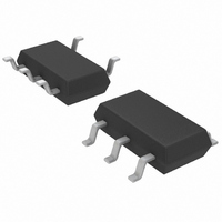
LT6650HS5#TRMPBF Linear Technology, LT6650HS5#TRMPBF Datasheet - Page 8

LT6650HS5#TRMPBF
Manufacturer Part Number
LT6650HS5#TRMPBF
Description
IC REF 400MV R-R BUFFER TSOT23-5
Manufacturer
Linear Technology
Datasheet
1.LT6650CS5TR.pdf
(12 pages)
Specifications of LT6650HS5#TRMPBF
Reference Type
Series
Voltage - Output
400mV
Tolerance
±1.5%
Temperature Coefficient
30ppm/°C
Voltage - Input
1.4 ~ 18 V
Number Of Channels
1
Current - Quiescent
11µA
Current - Output
200µA
Operating Temperature
-40°C ~ 125°C
Mounting Type
Surface Mount
Package / Case
TSOT-23-5, TSOT-5, TSOP-5
Lead Free Status / RoHS Status
Lead free / RoHS Compliant
Current - Cathode
-
Other names
LT6650HS5#PBF
LT6650HS5#PBF
LT6650HS5#PBF
Available stocks
Company
Part Number
Manufacturer
Quantity
Price
APPLICATIO S I FOR ATIO
LT6650
operated from a small battery or other relatively high
impedance source, a minimum 1µF capacitor is recom-
mended. PSRR can be significantly enhanced by adding a
low-pass RC filter on the input, with a time-constant of
1ms or higher, as shown in Figure 1. The Typical Perfor-
mance Characteristics graphs show performance as a
function of several combinations of input and output
capacitance.
An input RC of 100ms or more is recommended (such as
5k and 22µF) when output transients must be minimized
in the face of high supply noise, such as in automotive
applications. Figure 2 shows an input filter structure that
effectively eliminates supply transients from affecting the
output. With this extra input decoupling and the LT6650
operating normally from a 12V bus, 50V transients induce
less than <0.5% V
Figure 3 shows the turn-on response time for the circuit in
Figure 1. The input voltage steps from 0V to 3V, and the
output is configured to produce 400mV. Input bypass and
output load capacitance are 1µF, R
the output settles in approximately 0.5ms. Figure 4 shows
8
V
3V
0V
Figure 2. High Noise-Immunity Input Network
IN
Figure 3. LT6650 Turn-On Characteristic
POWER BUS
NOISY
OUT
33k
U
1µF
perturbations.
0.2ms/DIV
U
1N751
5V
4.7k
6650 F02
IN
W
= 0Ω, R
22µF
V
IN
6650 F03
Z
= 0Ω, and
U
V
0.4V
0V
OUT
the same circuit responding to input transients of 0.5V,
settling in about 0.3ms. Figures 5 through 7 show the
same circuit responding to various load steps: changes
between ±100µA in Figure 5; sourcing current step be-
tween –100µA and –200µA in Figure 6; and sinking current
SOURCING
SOURCING
10mV/DIV
10mV/DIV
Figure 6. Output Response to Current-Sourcing Load Step
(–100µA to –200µA)
SINKING
SINKING
–100µA
–200µA
Figure 5. Output Response to Bidirectional Load Step
(100µA to –100µA)
100µA
100µA
V
V
2.5V
0.4V
V
I
I
OUT
OUT
OUT
V
OUT
OUT
3V
0V
AC
Figure 4. Output Response to ±0.5V Input Step
IN
2ms/DIV
6650 F04
6650 F06
6650 F05
6650fa


